ZHCSI59I July   2009  – May 2018 TPS65070 , TPS65072 , TPS65073 , TPS650731 , TPS650732

UNLESS OTHERWISE NOTED, this document contains PRODUCTION DATA.  

  1. 特性
  2. 应用
  3. 说明
    1.     方框图
  4. 修订历史记录
  5. 说明 (续)
  6. Device Options
  7. Pin Configuration and Functions
    1.     Pin Functions
  8. Specifications
    1. 8.1  Absolute Maximum Ratings
    2. 8.2  ESD Ratings
    3. 8.3  Recommended Operating Conditions
    4. 8.4  Thermal Information
    5. 8.5  Electrical Characteristics
    6. 8.6  Electrical Characteristics - DCDC1 Converter
    7. 8.7  Electrical Characteristics - DCDC2 Converter
    8. 8.8  Electrical Characteristics - DCDC3 Converter
    9. 8.9  Electrical Characteristics - VLDO1 and VLDO2 Low Dropout Regulators
    10. 8.10 Electrical Characteristics - wLED Boost Converter
    11. 8.11 Electrical Characteristics - Reset, PB_IN, PB_OUT, PGood, Power_on, INT, EN_EXTLDO, EN_wLED
    12. 8.12 Electrical Characteristics - ADC Converter
    13. 8.13 Electrical Characteristics - Touch Screen Interface
    14. 8.14 Electrical Characteristics - Power Path
    15. 8.15 Electrical Characteristics - Battery Charger
    16. 8.16 Timing Requirements
    17. 8.17 Dissipation Ratings
    18. 8.18 Typical Characteristics
  9. Parameter Measurement Information
  10. 10Detailed Description
    1. 10.1 Overview
    2. 10.2 Functional Block Diagram
    3. 10.3 Feature Description
      1. 10.3.1  Battery Charger and Power Path
      2. 10.3.2  Power Down
      3. 10.3.3  Power-On Reset
      4. 10.3.4  Power-Path Management
        1. 10.3.4.1 SYS Output
      5. 10.3.5  Battery Charging
        1. 10.3.5.1 I-PRECHARGE
        2. 10.3.5.2 ITERM
        3. 10.3.5.3 Battery Detection and Recharge
        4. 10.3.5.4 Charge Termination On/Off
        5. 10.3.5.5 Timers
        6. 10.3.5.6 Dynamic Timer Function
        7. 10.3.5.7 Timer Fault
      6. 10.3.6  Battery Pack Temperature Monitoring
      7. 10.3.7  Battery Charger State Diagram
      8. 10.3.8  DC-DC Converters and LDOs
        1. 10.3.8.1 Operation
        2. 10.3.8.2 DCDC1 Converter
        3. 10.3.8.3 DCDC2 Converter
        4. 10.3.8.4 DCDC3 Converter
      9. 10.3.9  Power Save Mode
        1. 10.3.9.1 Dynamic Voltage Positioning
        2. 10.3.9.2 100% Duty Cycle Low Dropout Operation
        3. 10.3.9.3 Undervoltage Lockout
      10. 10.3.10 Short-Circuit Protection
        1. 10.3.10.1 Soft Start
      11. 10.3.11 Enable
        1. 10.3.11.1 RESET (TPS65070, TPS65073, TPS650731, TPS650732 Only)
        2. 10.3.11.2 PGOOD (Reset Signal For Applications Processor)
        3. 10.3.11.3 PB_IN (Push-Button IN)
        4. 10.3.11.4 PB_OUT
        5. 10.3.11.5 POWER_ON
        6. 10.3.11.6 EN_wLED (TPS65072 Only)
        7. 10.3.11.7 EN_EXTLDO (TPS65072 Only)
      12. 10.3.12 Short-Circuit Protection
      13. 10.3.13 Thermal Shutdown
        1. 10.3.13.1 Low Dropout Voltage Regulators
        2. 10.3.13.2 White LED Boost Converter
        3. 10.3.13.3 A/D Converter
        4. 10.3.13.4 Touch Screen Interface (only for TPS65070, TPS65073, TPS650731, TPS650732)
          1. 10.3.13.4.1 Performing Measurements Using the Touch Screen Controller
    4. 10.4 Device Functional Modes
    5. 10.5 Programming
      1. 10.5.1 I2C Interface Specification
        1. 10.5.1.1 Serial interface
    6. 10.6 Register Maps
      1. 10.6.1  PPATH1. Register Address: 01h
      2. 10.6.2  INT. Register Address: 02h
      3. 10.6.3  CHGCONFIG0. Register Address: 03h
      4. 10.6.4  CHGCONFIG1. Register Address: 04h
      5. 10.6.5  CHGCONFIG2. Register Address: 05h
      6. 10.6.6  CHGCONFIG3. Register Address: 06h
      7. 10.6.7  ADCONFIG. Register Address: 07h
      8. 10.6.8  TSCMODE. Register Address: 08h
      9. 10.6.9  ADRESULT_1. Register Address: 09h
      10. 10.6.10 ADRESULT_2. Register Address: 0Ah
      11. 10.6.11 PGOOD. Register Address: 0Bh
      12. 10.6.12 PGOODMASK. Register Address: 0Ch
      13. 10.6.13 CON_CTRL1. Register Address: 0Dh
      14. 10.6.14 CON_CTRL2. Register Address: 0Eh
      15. 10.6.15 CON_CTRL3. Register Address: 0Fh
      16. 10.6.16 DEFDCDC1. Register Address: 10h
      17. 10.6.17 DEFDCDC2_LOW. Register Address: 11h
      18. 10.6.18 DEFDCDC2_HIGH. Register Address: 12h
      19. 10.6.19 DEFDCDC3_LOW. Register Address: 13h
      20. 10.6.20 DEFDCDC3_HIGH. Register Address: 14h
      21. 10.6.21 DEFSLEW. Register Address: 15h
      22. 10.6.22 LDO_CTRL1. Register Address: 16h
      23. 10.6.23 DEFLDO2. Register Address: 17h
      24. 10.6.24 WLED_CTRL1. Register Address: 18h
      25. 10.6.25 WLED_CTRL2. Register Address: 19h
  11. 11Application and Implementation
    1. 11.1 Application Information
      1. 11.1.1 Power Solutions For Different Application Processors
        1. 11.1.1.1 Default Settings
        2. 11.1.1.2 Starting TPS6507x
    2. 11.2 Typical Applications
      1. 11.2.1 General PMIC Application
        1. 11.2.1.1 Design Requirements
        2. 11.2.1.2 Detailed Design Procedure
          1. 11.2.1.2.1 Output Filter Design (Inductor and Output Capacitor)
            1. 11.2.1.2.1.1 Inductor Selection
            2. 11.2.1.2.1.2 Output Capacitor Selection
            3. 11.2.1.2.1.3 Input Capacitor Selection/Input Voltage
            4. 11.2.1.2.1.4 Output Voltage Selection
            5. 11.2.1.2.1.5 Voltage Change on DCDC2 and DCDC3
          2. 11.2.1.2.2 LDOs
            1. 11.2.1.2.2.1 Output Capacitor Selection
            2. 11.2.1.2.2.2 Input Capacitor Selection
            3. 11.2.1.2.2.3 Output Voltage Change For LDO1 and LDO2
            4. 11.2.1.2.2.4 Unused LDOs
          3. 11.2.1.2.3 White-LED Boost Converter
            1. 11.2.1.2.3.1 LED-Current Setting/Dimming
            2. 11.2.1.2.3.2 Setup
            3. 11.2.1.2.3.3 Setting the LED Current
            4. 11.2.1.2.3.4 Inductor Selection
            5. 11.2.1.2.3.5 Diode Selection
            6. 11.2.1.2.3.6 Output Capacitor Selection
            7. 11.2.1.2.3.7 Input Capacitor Selection
          4. 11.2.1.2.4 Battery Charger
            1. 11.2.1.2.4.1 Temperature Sensing
            2. 11.2.1.2.4.2 Changing the Charging Temperature Range (Default 0°C to 45°C)
        3. 11.2.1.3 Application Curves
      2. 11.2.2 Powering OMAP-L138
        1. 11.2.2.1 Design Requirements
        2. 11.2.2.2 Detailed Design Procedure
      3. 11.2.3 Powering Atlas IV
        1. 11.2.3.1 Design Requirements
        2. 11.2.3.2 Detailed Design Procedure
          1. 11.2.3.2.1 Prima SLEEP Mode and DEEP SLEEP Mode Support
          2. 11.2.3.2.2 SLEEP Mode
          3. 11.2.3.2.3 DEEP SLEEP Mode
      4. 11.2.4 OMAP35xx (Supporting SYS-OFF Mode)
        1. 11.2.4.1 Design Requirements
        2. 11.2.4.2 Detailed Design Procedure
      5. 11.2.5 TPS650731 for OMAP35xx
        1. 11.2.5.1 Design Requirements
        2. 11.2.5.2 Detailed Design Procedure
      6. 11.2.6 Powering AM3505 Using TPS650732
        1. 11.2.6.1 Design Requirements
        2. 11.2.6.2 Detailed Design Procedure
  12. 12Power Supply Recommendations
  13. 13Layout
    1. 13.1 Layout Guidelines
    2. 13.2 Layout Example
  14. 14器件和文档支持
    1. 14.1 器件支持
      1. 14.1.1 第三方米6体育平台手机版_好二三四免责声明
    2. 14.2 文档支持
      1. 14.2.1 相关文档
    3. 14.3 相关链接
    4. 14.4 接收文档更新通知
    5. 14.5 社区资源
    6. 14.6 商标
    7. 14.7 静电放电警告
    8. 14.8 术语表
  15. 15机械、封装和可订购信息

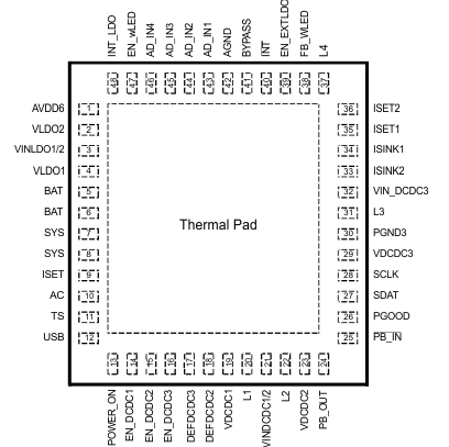
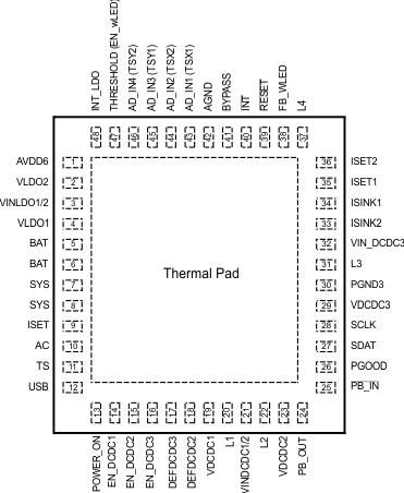
Pin Configuration and Functions

TPS6507x RSL Package
48-Pin VQFN With Thermal Pad
Top View
TPS65070 TPS65072 TPS65073 TPS650731 TPS650732 pos2_lvs950.gif
TPS65072 RSL Package
48-Pin VQFN With Thermal Pad
Top View
TPS65070 TPS65072 TPS65073 TPS650731 TPS650732 pos1_lvs950.gif

Pin Functions

PIN I/O DESCRIPTION
NAME NO.
TPS6507x TPS65072
CHARGER BLOCK
AC 10 10 I Input power for power path manager, connect to external DC supply. Connect external 1 µF (minimum) to GND
AD_IN1 (TSX1) 43 43 I Analog input1 for A/D converter;
TPS65070, TPS65073, TPS650731, TPS650732 only:
Input 1 to the x-plate for the touch screen.
AD_IN2 (TSX2) 44 44 I Analog input2 for A/D converter;
TPS65070, TPS65073, TPS650731, TPS650732 only:

Input 2 to the x-plate for the touch screen
AD_IN3 (TSY1) 45 45 I Analog input3 for A/D converter;
TPS65070, TPS65073, TPS650731, TPS650732 only:
Input 1 to the y-plate for the touch screen
AD_IN4 (TSY2) 46 46 I Analog input4 for A/D converter;
TPS65070, TPS65073, TPS650731, TPS650732 only:

Input 2 to the y-plate for the touch screen
AVDD6 1 1 O Internal “always-on”-voltage. Connect a 4.7-µF capacitor from AVDD6 to GND
BAT 5, 6 5, 6 O Charger power stage output, connect to battery. Place a ceramic capacitor of 10 µF from these pins to GND
BYPASS 41 41 O Connect a 10-µF bypass capacitor from this pin to GND. This pin can optionally be used as a reference output (2.26 V). The maximum load on this pin is 0.1 mA.
INT 40 40 O Open-drain interrupt output. An interrupt can be generated upon:
• A touch of the touch screen
• Voltage applied or removed at pins AC or USB
PB_IN actively pulled low (optionally actively pulled high)
INT_LDO 48 48 O Connect a 2.2-µF bypass capacitor from this pin to GND. The pin is connected to an internal LDO providing the power for the touch screen controller (TSREF).
ISET 9 9 I Connect a resistor from ISET to GND to set the charge current.
SCLK 28 28 I Clock input for the I2C interface.
SDAT 27 27 I/O Data line for the I2C interface.
SYS 7, 8 7, 8 O System voltage; output of the power path manager. All voltage regulators are typically powered from this output.
TS 11 11 I Temperature sense input. Connect to NTC thermistor to sense battery pack temperature. TPS6507x can be internally programmed to operate with a 10-kΩ curve 2 or 100-kΩ curve 1 thermistor. To linearize the thermistor response, use a 75-kΩ (for the 10-kΩ NTC) or a 360-kΩ (for the 100-kΩ NTC) in parallel with the thermistor. Default setting is 10-kΩ NTC.
USB 12 12 I Input power for power path manager, connect to external voltage from a USB port. Connect external 1 µF (minimum) to GND. Default input current limit is 500 mA maximum.
CONVERTERS
AGND 42 42 Analog GND, connect to PGND (thermal pad)
DEFDCDC2 18 18 I Select Pin of DCDC2 output voltage.
DEFDCDC3 17 17 I Select Pin of DCDC3 output voltage.
EN_DCDC1 14 14 I Enable Input for DCDC1, active high
EN_DCDC2 15 15 I Enable Input for DCDC2, active high
EN_DCDC3 16 16 I Enable Input for DCDC3, active high
EN_EXTLDO 39 O TPS65072:
This pin is the active high, push-pull output to enable an external LDO. This pin will be set and reset during startup and shutdown by the sequencing option programmed. The output is pulled internally to the SYS voltage if HIGH.
The output is only used for sequencing options for Sirf Prima or Atlas 4 processors with DCDC_SQ[2..0] = 100 or DCDC_SQ[2..0] = 111.
EN_wLED 47 I TPS65072, : This pin is the actively high enable input for the wLED driver. The wLED converter is enabled by the ENABLE ISINK Bit OR enable EN_wLED pin.
FB_WLED 38 38 I Feedback input for the boost converter's output voltage.
ISET1
(AD_IN6)
35 35 I Connect a resistor from this pin to GND to set the full scale current for Isink1 and Isink2 with Bit Current Level in register WLED_CTRL0 set to 1.
Analog input6 for the A/D converter.
ISET2
(AD_IN7)
36 36 I Connect a resistor from this pin to GND to set the full scale current for Isink1 and Isink2 with Bit Current Level in register WLED_CTRL0 set to 0.
Analog input7 for the A/D converter.
ISINK1 34 34 I Input to the current sink 1. Connect the cathode of the LEDs to this pin.
ISINK2 33 33 I Input to the current sink 2. Connect the cathode of the LEDs to this pin.
L1 20 20 O Switch Pin for DCDC1. Connect to Inductor
L2 22 22 O Switch Pin of DCDC2. Connect to Inductor.
L3 31 31 O Switch Pin of DCDC3. Connect to Inductor.
L4 37 37 I Switch Pin of the white LED (wLED) boost converter. Connect to Inductor and rectifier diode.
PB_IN 25 25 I Enable input for TPS6507x. When pulled LOW, the DCDC converters and LDOs start with the sequencing as programmed internally. Internal 50kO pullup resistor to AVDD6
PB_OUT 24 24 O Open-drain output. This pin is driven by the status of the /PB_IN input (after debounce). PB_OUT=LOW if PB_IN=LOW
PGND3 30 30 Power GND for DCDC3. Connect to PGND (thermal pad)
PGOOD 26 26 O Open-drain power good output. The delay time equals the setting for Reset. The pin will go low depending on the setting in register PGOODMASK. Optionally it is also driven LOW for 0.5 ms when PB_IN is pulled LOW for >15s.
POWER_ON 13 13 I Power_ON input for the internal state machine. After PB_IN was pulled LOW to turn on the TPS6507x, the POWER_ON pin needs to be pulled HIGH by the application processor to keep the system in ON-state when PB_IN is released HIGH. If POWER_ON is released LOW, the DCDC converters and LDOs will turn off when PB_IN is HIGH.
RESET 39 O TPS65070, TPS65073, TPS650731, TPS650732:
Open-drain active low reset output, reset delay time equals settings in register PGOOD. The status depends on the voltage applied at THRESHOLD.
THRESHOLD 47 I TPS65070, TPS65073, TPS650731, TPS650732:Input for the reset comparator. RESET will be LOW if this voltage drops below 1 V.
VDCDC1 19 19 I Feedback voltage sense input. For the fixed voltage option, this pin must directly be connected to Vout1, for the adjustable version, this pin is connected to an external resistor divider.
VDCDC2 23 23 I Feedback voltage sense input, connect directly to Vout2
VDCDC3 29 29 I Feedback voltage sense input, connect directly to Vout3
VINDCDC1/2 21 21 I Input voltage for DCDC1 and DCDC2 step-down converter. This pin must be connected to the SYS pin.
VINLDO1/2 3 3 I Input voltage for LDO1 and LDO2
VIN_DCDC3 32 32 I Input voltage for DCDC3 step-down converter. This pin must be connected to the SYS pin.
VLDO1 4 4 O Output voltage of LDO1
VLDO2 2 2 O Output voltage of LDO2
Thermal Pad Power ground connection for the PMU. Connect to GND