ZHCSI67D May 2018 – December 2019 MSP430FR2153 , MSP430FR2155 , MSP430FR2353 , MSP430FR2355
PRODUCTION DATA.
- 1器件概述
- 2Device Comparison
- 3Terminal Configuration and Functions
-
4Specifications
- 4.1 Absolute Maximum Ratings
- 4.2 ESD Ratings
- 4.3 Recommended Operating Conditions
- 4.4 Active Mode Supply Current Into VCC Excluding External Current
- 4.5 Active Mode Supply Current Per MHz
- 4.6 Low-Power Mode LPM0 Supply Currents Into VCC Excluding External Current
- 4.7 Low-Power Mode LPM3 and LPM4 Supply Currents (Into VCC) Excluding External Current
- 4.8 Low-Power Mode LPMx.5 Supply Currents (Into VCC) Excluding External Current
- 4.9 Production Distribution of LPM Supply Currents
- 4.10 Typical Characteristics - Current Consumption Per Module
- 4.11 Thermal Resistance Characteristics
- 4.12
Timing and Switching Characteristics
- 4.12.1 Power Supply Sequencing
- 4.12.2 Reset Timing
- 4.12.3 Clock Specifications
- 4.12.4 Internal Shared Reference
- 4.12.5 General-Purpose I/Os
- 4.12.6 Digital I/O Typical Characteristics
- 4.12.7 Timer_B
- 4.12.8
eUSCI
- Table 4-14 eUSCI (UART Mode) Clock Frequencies
- Table 4-15 eUSCI (UART Mode) Switching Characteristics
- Table 4-16 eUSCI (SPI Master Mode) Clock Frequency
- Table 4-17 eUSCI (SPI Master Mode) Switching Characteristics
- Table 4-18 eUSCI (SPI Slave Mode) Switching Characteristics
- Table 4-19 eUSCI (I2C Mode) Switching Characteristics
- 4.12.9 ADC
- 4.12.10 Enhanced Comparator (eCOMP)
- 4.12.11 Smart Analog Combo (SAC) (MSP430FR235x Devices Only)
- 4.12.12 FRAM
- 4.12.13 Emulation and Debug
-
5Detailed Description
- 5.1 CPU
- 5.2 Operating Modes
- 5.3 Interrupt Vector Addresses
- 5.4 Memory Organization
- 5.5 Bootloader (BSL)
- 5.6 JTAG Standard Interface
- 5.7 Spy-Bi-Wire Interface (SBW)
- 5.8 FRAM
- 5.9 Memory Protection
- 5.10
Peripherals
- 5.10.1 Power Management Module (PMM) and On-Chip Reference Voltages
- 5.10.2 Clock System (CS) and Clock Distribution
- 5.10.3 General-Purpose Input/Output Port (I/O)
- 5.10.4 Watchdog Timer (WDT)
- 5.10.5 System Module (SYS)
- 5.10.6 Cyclic Redundancy Check (CRC)
- 5.10.7 Interrupt Compare Controller (ICC)
- 5.10.8 Enhanced Universal Serial Communication Interface (eUSCI_A0, eUSCI_A1, eUSCI_B0, eUSCI_B1)
- 5.10.9 Timers (Timer0_B3, Timer1_B3, Timer2_B3, Timer3_B7)
- 5.10.10 Backup Memory (BKMEM)
- 5.10.11 Real-Time Clock (RTC) Counter
- 5.10.12 12-Bit Analog-to-Digital Converter (ADC)
- 5.10.13 Enhanced Comparator
- 5.10.14 Manchester Function Module (MFM)
- 5.10.15 Smart Analog Combo (SAC) (MSP430FR235x Devices Only)
- 5.10.16 eCOMP0, eCOMP1, SAC0, SAC1, SAC2, and SAC3 Interconnection (MSP430FR235x Devices Only)
- 5.10.17 Cross-Chip Interconnection (SACx are MSP430FR235x Devices Only)
- 5.10.18 Embedded Emulation Module (EEM)
- 5.10.19 Peripheral File Map
- 5.11 Input/Output Diagrams
- 5.12 Device Descriptors (TLV)
- 5.13 Identification
- 6Applications, Implementation, and Layout
- 7器件和文档支持
- 8机械、封装和可订购信息
6.1.3 JTAG
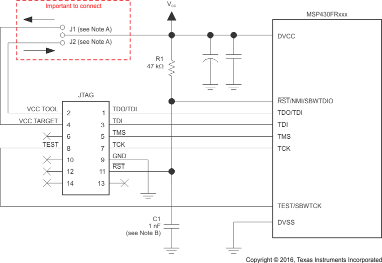
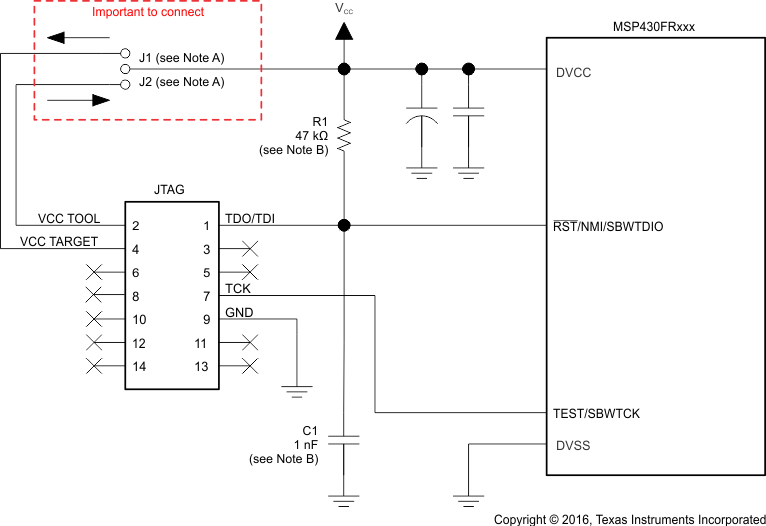
With the proper connections, the debugger and a hardware JTAG interface (such as the MSP-FET or MSP-FET430UIF) can be used to program and debug code on the target board. In addition, the connections also support the MSP-GANG production programmers, thus providing an easy way to program prototype boards, if desired. Figure 6-3 shows the connections between the 14-pin JTAG connector and the target device required to support in-system programming and debugging for 4-wire JTAG communication. Figure 6-4 shows the connections for 2-wire JTAG mode (Spy-Bi-Wire).
The connections for the MSP-FET and MSP-FET430UIF interface modules and the MSP-GANG are identical. Both can supply VCC to the target board (through pin 2). In addition, the MSP-FET and MSP-FET430UIF interface modules and MSP-GANG have a VCC sense feature that, if used, requires an alternate connection (pin 4 instead of pin 2). The VCC-sense feature senses the local VCC present on the target board (that is, a battery or other local power supply) and adjusts the output signals accordingly. Figure 6-3 and Figure 6-4 show a jumper block that supports both scenarios of supplying VCC to the target board. If this flexibility is not required, the desired VCC connections can be hard-wired to eliminate the jumper block. Pins 2 and 4 must not be connected at the same time.
For additional design information regarding the JTAG interface, see the MSP430 hardware tools user’s guide.

