ZHCSI81L February 2009 – May 2018 LM26420
PRODUCTION DATA.
- 1 特性
- 2 应用
- 3 说明
- 4 修订历史记录
- 5 Pin Configuration and Functions
- 6 Specifications
- 7 Detailed Description
-
8 Application and Implementation
- 8.1 Application Information
- 8.2
Typical Applications
- 8.2.1 LM26420X 2.2-MHz, 0.8-V Typical High-Efficiency Application Circuit
- 8.2.2 LM26420X 2.2-MHz, 1.8-V Typical High-Efficiency Application Circuit
- 8.2.3 LM26420X 2.2-MHz, 2.5-V Typical High-Efficiency Application Circuit
- 8.2.4 LM26420Y 550 kHz, 0.8-V Typical High-Efficiency Application Circuit
- 8.2.5 LM26420Y 550-kHz, 1.8-V Typical High-Efficiency Application Circuit
- 8.2.6 LM26420Y 550-kHz, 2.5-V Typical High-Efficiency Application Circuit
- 9 Power Supply Recommendations
- 10Layout
- 11器件和文档支持
- 12机械、封装和可订购信息
7.1 Overview
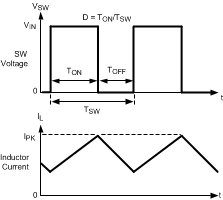
The LM26420 is a constant frequency dual PWM buck synchronous regulator device that can supply two loads at up to 2 A each. The regulator has a preset switching frequency of either 2.2 MHz or 550 kHz. This high frequency allows the LM26420 to operate with small surface mount capacitors and inductors, resulting in a DC/DC converter that requires a minimum amount of board space. The LM26420 is internally compensated, so it is simple to use and requires few external components. The LM26420 uses current-mode control to regulate the output voltage. The following operating description of the LM26420 refers to the Functional Block Diagram, which depicts the functional blocks for one of the two channels, and to the waveforms in Figure 27. The LM26420 supplies a regulated output voltage by switching the internal PMOS and NMOS switches at constant frequency and variable duty cycle. A switching cycle begins at the falling edge of the reset pulse generated by the internal clock. When this pulse goes low, the output control logic turns on the internal PMOS control switch (TOP Switch). During this on-time, the SW pin voltage (VSW) swings up to approximately VIN, and the inductor current (IL) increases with a linear slope. IL is measured by the current sense amplifier, which generates an output proportional to the switch current. The sense signal is summed with the regulator’s corrective ramp and compared to the error amplifier’s output, which is proportional to the difference between the feedback voltage and VREF. When the PWM comparator output goes high, the TOP Switch turns off and the NMOS switch (BOTTOM Switch) turns on after a short delay, which is controlled by the Dead-Time-Control Logic, until the next switching cycle begins. During the top switch off-time, inductor current discharges through the BOTTOM Switch, which forces the SW pin to swing to ground. The regulator loop adjusts the duty cycle (D) to maintain a constant output voltage.
 Figure 27. LM26420 Basic Operation of the PWM Comparator