ZHCSI81L February 2009 – May 2018 LM26420
PRODUCTION DATA.
- 1 特性
- 2 应用
- 3 说明
- 4 修订历史记录
- 5 Pin Configuration and Functions
- 6 Specifications
- 7 Detailed Description
-
8 Application and Implementation
- 8.1 Application Information
- 8.2
Typical Applications
- 8.2.1 LM26420X 2.2-MHz, 0.8-V Typical High-Efficiency Application Circuit
- 8.2.2 LM26420X 2.2-MHz, 1.8-V Typical High-Efficiency Application Circuit
- 8.2.3 LM26420X 2.2-MHz, 2.5-V Typical High-Efficiency Application Circuit
- 8.2.4 LM26420Y 550 kHz, 0.8-V Typical High-Efficiency Application Circuit
- 8.2.5 LM26420Y 550-kHz, 1.8-V Typical High-Efficiency Application Circuit
- 8.2.6 LM26420Y 550-kHz, 2.5-V Typical High-Efficiency Application Circuit
- 9 Power Supply Recommendations
- 10Layout
- 11器件和文档支持
- 12机械、封装和可订购信息
8.1.3 Using Precision Enable and Power Good
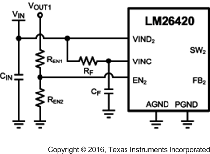
The LM26420 device precision EN and PG pins address many of the sequencing requirements required in today's challenging applications. Each output can be controlled independently and have independent power good. This allows for a multitude of ways to control each output. Typically, the enables to each output are tied together to the input voltage and the outputs ratiometrically ramp up when the input voltage reaches above UVLO rising threshold. There may be instances where it is desired that the second output (VOUT2) does not turn on until the first output (VOUT1) has reached 90% of the desired setpoint. This is easily achieved with an external resistor divider attached from VOUT1 to EN2, see Figure 31.
 Figure 31. VOUT1 Controlling VOUT2 with Resistor Divider
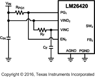
 If it is not desired to have a resistor divider to control VOUT2 with VOUT1, then the PG1 can be connected to the EN2 pin to control VOUT2, see Figure 32. RPG1 is a pullup resistor on the range of 10 kΩ to 100 kΩ, 50 kΩ is the suggested value. This turns on VOUT2 when VOUT1 is approximately 90% of the programmed output.
NOTE
This also turns off VOUT2 when VOUT1 is outside the ±10% of the programmed output.
 Figure 32. PG1 Controlling VOUT2
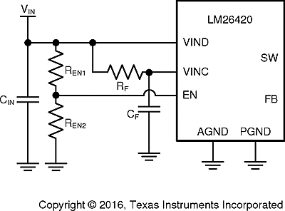
 Another example might be that the output is not to be turned on until the input voltage reaches 90% of desired voltage setpoint. This verifies that the input supply is stable before turning on the output. Select REN1 and REN2 such that the voltage at the EN pin is greater than 1.12 V when reaching the 90% desired set-point.
 Figure 33. VOUT Controlling VIN
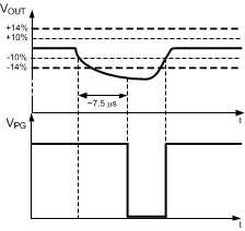
 The power good feature of the LM26420 is designed with hysteresis in order to ensure no false power good flags are asserted during large transient. Once power good is asserted high, it is not pulled low until the output voltage exceeds ±14% of the setpoint for a during of approximately 7.5 µs (typical), see Figure 34.
 Figure 34. Power Good Hysteresis Operation