ZHCSI90E December 2017 – October 2019 ISO1042
PRODUCTION DATA.
- 1 特性
- 2 应用
- 3 说明
- 4 修订历史记录
- 5 Pin Configuration and Functions
-
6 Specifications
- 6.1 Absolute Maximum Ratings
- 6.2 ESD Ratings
- 6.3 Transient Immunity
- 6.4 Recommended Operating Conditions
- 6.5 Thermal Information
- 6.6 Power Ratings
- 6.7 Insulation Specifications
- 6.8 Safety-Related Certifications
- 6.9 Safety Limiting Values
- 6.10 Electrical Characteristics - DC Specification
- 6.11 Switching Characteristics
- 6.12 Insulation Characteristics Curves
- 6.13 Typical Characteristics
- 7 Parameter Measurement Information
- 8 Detailed Description
- 9 Application and Implementation
- 10Power Supply Recommendations
- 11Layout
- 12器件和文档支持
- 13机械、封装和可订购信息
7.1 Test Circuits
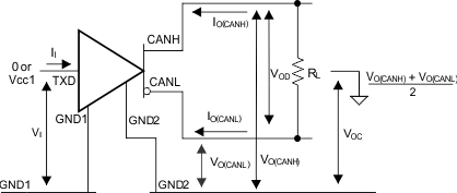 Figure 15. Driver Voltage, Current and Test Definitions
  Figure 16. Bus Logic State Voltage Definitions
A. The input pulse is supplied by a generator having the following characteristics: PRR ≤ 125 kHz, 50% duty cycle,
tr ≤ 6 ns, tf ≤ 6 ns, ZO = 50 Ω.
Figure 17. Driver Test Circuit and Voltage Waveforms tr ≤ 6 ns, tf ≤ 6 ns, ZO = 50 Ω.
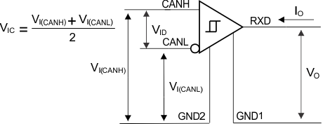 Figure 18. Receiver Voltage and Current Definitions
A. The input pulse is supplied by a generator having the following characteristics: PRR ≤ 125 kHz, 50% duty cycle,
tr ≤ 6 ns, tf ≤ 6 ns, ZO = 50 Ω.
Figure 19. Receiver Test Circuit and Voltage Waveforms tr ≤ 6 ns, tf ≤ 6 ns, ZO = 50 Ω.
Table 1. Receiver Differential Input Voltage Threshold Test
| INPUT | OUTPUT | |||
|---|---|---|---|---|
| VCANH | VCANL | |VID| | RXD | |
| -29.5 V | -30.5 V | 1000 mV | L | VOL |
| 30.5 V | 29.5 V | 1000 mV | L | |
| -19.55 V | -20.45 V | 900 mV | L | |
| 20.45 V | 19.55 V | 900 mV | L | |
| -19.75 V | -20.25 V | 500 mV | H | VOH |
| 20.25 V | 19.75 V | 500 mV | H | |
| -29.8 V | -30.2 V | 400 mV | H | |
| 30.2 V | 29.8 V | 400 mV | H | |
| Open | Open | X | H | |
 Figure 20. tLOOP Test Circuit and Voltage Waveforms
 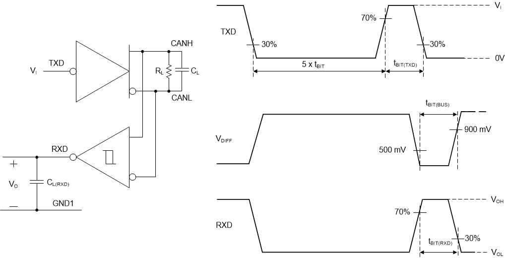 Figure 21. CAN FD Timing Parameter Measurement
A. The input pulse is supplied by a generator having the following characteristics: tr ≤ 6 ns, tf ≤ 6 ns, ZO = 50 Ω.
Figure 22. Dominant Time-out Test Circuit and Voltage Waveforms 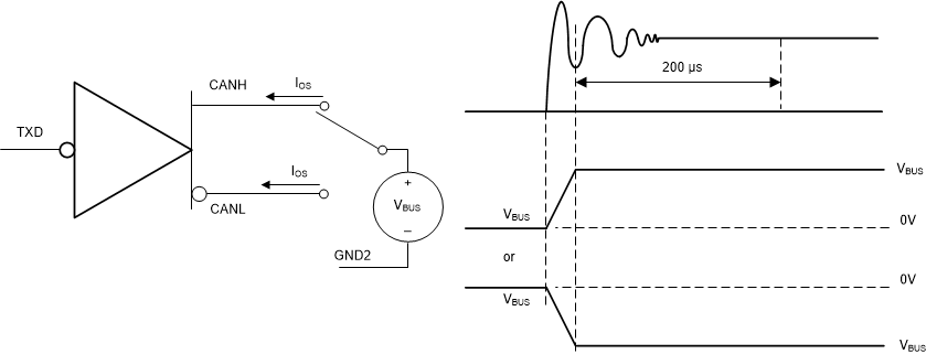 Figure 23. Driver Short-Circuit Current Test Circuit and Waveforms
 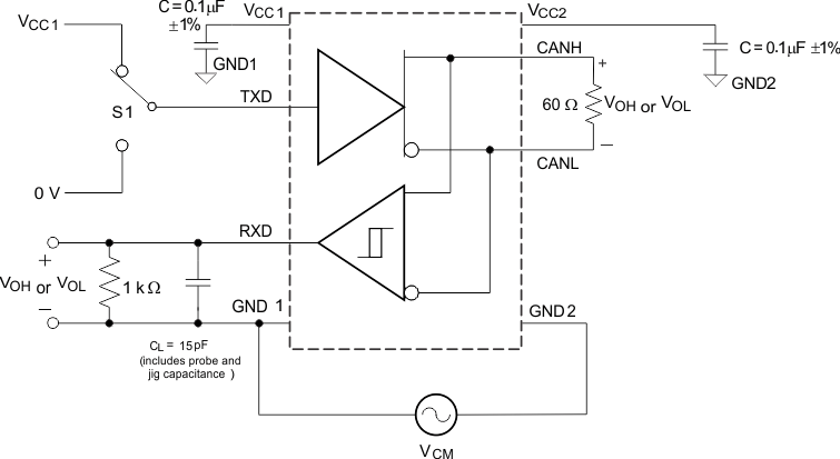 Figure 24. Common-Mode Transient Immunity Test Circuit