ZHCSIA5A July 2018 – December 2018 INA253
PRODUCTION DATA.
- 1 特性
- 2 应用
- 3 说明
- 4 修订历史记录
- 5 Device Comparison Table
- 6 Pin Configuration and Functions
- 7 Specifications
-
8 Detailed Description
- 8.1 Overview
- 8.2 Functional Block Diagram
- 8.3 Feature Description
- 8.4
Device Functional Modes
- 8.4.1 Adjusting the Output Midpoint With the Reference Pins
- 8.4.2 Reference Pin Connections for Unidirectional Current Measurements
- 8.4.3 Ground Referenced Output
- 8.4.4 Reference Pin Connections for Bidirectional Current Measurements
- 8.4.5 Output Set to Mid-Supply Voltage
- 8.4.6 Output Set to Mid-External Reference
- 8.4.7 Output Set Using Resistor Divide
- 9 Application and Implementation
- 10Power Supply Recommendations
- 11Layout
- 12器件和文档支持
- 13机械、封装和可订购信息
8.4.7 Output Set Using Resistor Divide
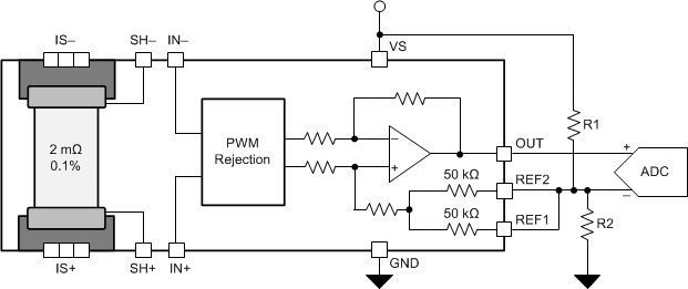
The INA253 REF1 and REF2 pins allow for the midpoint of the output voltage to be adjusted for system circuitry connections to analog to digital converters (ADCs) or other amplifiers. The REF pins are designed to be connected directly to supply, ground, or a low-impedance reference voltage. The REF pins can be connected together and biased using a resistor divider to achieve a custom output voltage. If the amplifier is used in this configuration, as shown in Figure 38, use the output as a differential signal with respect to the resistor divider voltage. For most accurate results, do not use single-ended measurements at the amplifier output because the internal impedance shifts can adversely affect device performance specifications.
 Figure 38. Setting the Reference Using a Resistor Divider