ZHCSIG5E July 2018 – August 2021 TPS63805 , TPS63806 , TPS63807
PRODUCTION DATA
- 1 特性
- 2 应用
- 3 说明
- 4 Revision History
- 5 说明(续)
- 6 Device Comparison Table
- 7 Pin Configuration and Functions
- 8 Specifications
-
9 Detailed Description
- 9.1 Overview
- 9.2 Functional Block Diagram
- 9.3
Feature Description
- 9.3.1 Control Loop Description
- 9.3.2 Precise Device Enable: Threshold- or Delayed Enable
- 9.3.3 Mode Selection (PFM/PWM)
- 9.3.4 Undervoltage Lockout (UVLO)
- 9.3.5 Soft Start
- 9.3.6 Adjustable Output Voltage
- 9.3.7 Overtemperature Protection - Thermal Shutdown
- 9.3.8 Input Overvoltage - Reverse-Boost Protection (IVP)
- 9.3.9 Output Overvoltage Protection (OVP)
- 9.3.10 Power-Good Indicator
- 9.4 Device Functional Modes
- 10Application and Implementation
- 11Power Supply Recommendations
- 12Layout
- 13Device and Documentation Support
- 14Mechanical, Packaging, and Orderable Information
9.3.2 Precise Device Enable: Threshold- or Delayed Enable
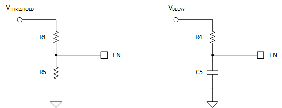
The enable-pin is a digital input to enable or disable the device by applying a high or low level. The device enters shutdown when EN is set low. In addition, this input features a precise threshold and can be used as a comparator that enables and disables the part at a defined threshold. This allows you to drive the state by a slowly changing voltage and enables the use of an external RC network to achieve a precise power-up delay. The enable pin can also be used with an external voltage divider to set a user-defined minimum supply voltage. For proper operation, the EN pin must be terminated and must not be left floating.
 Figure 9-2 Circuit Example for How to Use the Precise Device Enable Feature