ZHCSII0A July   2018  – November 2018 ADS1219

PRODUCTION DATA.  

  1. 特性
  2. 应用
  3. 说明
    1.     Device Images
      1.      电压、电流和温度监控应用
  4. 修订历史记录
  5. Pin Configuration and Functions
    1.     Pin Functions
  6. Specifications
    1. 6.1 Absolute Maximum Ratings
    2. 6.2 ESD Ratings
    3. 6.3 Recommended Operating Conditions
    4. 6.4 Thermal Information
    5. 6.5 Electrical Characteristics
    6. 6.6 I2C Timing Requirements
    7. 6.7 I2C Switching Characteristics
    8. 6.8 Typical Characteristics
  7. Parameter Measurement Information
    1. 7.1 Noise Performance
  8. Detailed Description
    1. 8.1 Overview
    2. 8.2 Functional Block Diagram
    3. 8.3 Feature Description
      1. 8.3.1 Multiplexer
      2. 8.3.2 Rail-to-Rail Input Buffers and Programmable Gain Stage
      3. 8.3.3 Voltage Reference
      4. 8.3.4 Modulator and Internal Oscillator
      5. 8.3.5 Digital Filter
      6. 8.3.6 Conversion Times
      7. 8.3.7 Offset Calibration
    4. 8.4 Device Functional Modes
      1. 8.4.1 Power-Up and Reset
        1. 8.4.1.1 Power-On Reset
        2. 8.4.1.2 RESET Pin
        3. 8.4.1.3 Reset by Command
      2. 8.4.2 Conversion Modes
        1. 8.4.2.1 Single-Shot Conversion Mode
        2. 8.4.2.2 Continuous Conversion Mode
      3. 8.4.3 Power-Down Mode
    5. 8.5 Programming
      1. 8.5.1 I2C Interface
        1. 8.5.1.1 I2C Address
        2. 8.5.1.2 Serial Clock (SCL) and Serial Data (SDA)
        3. 8.5.1.3 Data Ready (DRDY)
        4. 8.5.1.4 Interface Speed
        5. 8.5.1.5 Data Transfer Protocol
        6. 8.5.1.6 I2C General Call (Software Reset)
        7. 8.5.1.7 Timeout
      2. 8.5.2 Data Format
      3. 8.5.3 Commands
        1. 8.5.3.1 Command Latching
        2. 8.5.3.2 RESET (0000 011x)
        3. 8.5.3.3 START/SYNC (0000 100x)
        4. 8.5.3.4 POWERDOWN (0000 001x)
        5. 8.5.3.5 RDATA (0001 xxxx)
        6. 8.5.3.6 RREG (0010 0rxx)
        7. 8.5.3.7 WREG (0100 00xx dddd dddd)
      4. 8.5.4 Reading Data and Monitoring for New Conversion Results
    6. 8.6 Register Map
      1. 8.6.1 Configuration and Status Registers
      2. 8.6.2 Register Descriptions
        1. 8.6.2.1 Configuration Register (address = 0h) [reset = 00h]
          1. Table 10. Configuration Register Field Descriptions
        2. 8.6.2.2 Status Register (address = 1h) [reset = 00h]
          1. Table 11. Status Register Field Descriptions
  9. Application and Implementation
    1. 9.1 Application Information
      1. 9.1.1 Interface Connections
      2. 9.1.2 Connecting Multiple Devices on the Same I2C Bus
      3. 9.1.3 Unused Inputs and Outputs
      4. 9.1.4 Analog Input Filtering
      5. 9.1.5 External Reference and Ratiometric Measurements
      6. 9.1.6 Establishing Proper Limits on the Absolute Input Voltage
      7. 9.1.7 Pseudo Code Example
    2. 9.2 Typical Application
      1. 9.2.1 Design Requirements
      2. 9.2.2 Detailed Design Procedure
        1. 9.2.2.1 Voltage Monitoring
        2. 9.2.2.2 High-Side Current Measurement
        3. 9.2.2.3 Thermistor Measurement
        4. 9.2.2.4 Register Settings
      3. 9.2.3 Application Curve
  10. 10Power Supply Recommendations
    1. 10.1 Power-Supply Sequencing
    2. 10.2 Power-Supply Decoupling
  11. 11Layout
    1. 11.1 Layout Guidelines
    2. 11.2 Layout Example
  12. 12器件和文档支持
    1. 12.1 器件支持
      1. 12.1.1 第三方米6体育平台手机版_好二三四免责声明
    2. 12.2 文档支持
      1. 12.2.1 相关文档
    3. 12.3 接收文档更新通知
    4. 12.4 社区资源
    5. 12.5 商标
    6. 12.6 静电放电警告
    7. 12.7 术语表
  13. 13机械、封装和可订购信息

Data Format

The device provides 24 bits of data in binary two's complement format. Use Equation 5 to calculate the size of one code (LSB).

Equation 5. 1 LSB = (2 · VREF / Gain) / 224 = +FS / 223

A positive full-scale input [VIN ≥ (+FS – 1 LSB) = (VREF / Gain – 1 LSB)] produces an output code of 7FFFFFh and a negative full-scale input (VIN ≤ –FS = –VREF / Gain) produces an output code of 800000h. The output clips at these codes for signals that exceed full-scale.

Table 6 summarizes the ideal output codes for different input signals.

Table 6. Ideal Output Code versus Input Signal

INPUT SIGNAL,
VIN = VAINP – VAINN
IDEAL OUTPUT CODE(1)
≥ FS (223 – 1) / 223 7FFFFFh
FS / 223 000001h
0 000000h
–FS / 223 FFFFFFh
≤ –FS 800000h
Excludes the effects of noise, INL, offset, and gain errors.

Figure 35 shows the mapping of the analog input signal to the output codes.
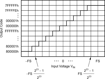
ADS1219 ai_code_transition_bas501.gifFigure 35. Code Transition Diagram

NOTE

Single-ended signal measurements, where VAINN = 0 V and VAINP = 0 V to +FS, only use the positive code range from 000000h to 7FFFFFh. However, because of device offset, the ADS1219 can still output negative codes when VAINP is close to 0 V.