ZHCSIJ3C June 2008 – July 2018 ADS7950 , ADS7951 , ADS7952 , ADS7953 , ADS7954 , ADS7955 , ADS7956 , ADS7957 , ADS7958 , ADS7959 , ADS7960 , ADS7961
PRODUCTION DATA.
- 1 特性
- 2 应用
- 3 说明
- 4 修订历史记录
- 5 器件比较表
- 6 Pin Configuration and Functions
-
7 Specifications
- 7.1 Absolute Maximum Ratings
- 7.2 ESD Ratings
- 7.3 Recommended Operating Conditions
- 7.4 Thermal Information: TSSOP
- 7.5 Thermal Information: VQFN
- 7.6 Electrical Characteristics: ADS7950, ADS7951, ADS7952, ADS7953
- 7.7 Electrical Characteristics, ADS7954, ADS7955, ADS7956, ADS7957
- 7.8 Electrical Characteristics, ADS7958, ADS7959, ADS7960, ADS7961
- 7.9 Timing Requirements
- 7.10 Typical Characteristics (All ADS79xx Family Devices)
- 7.11 Typical Characteristics (12-Bit Devices Only)
- 7.12 Typical Characteristics (12-Bit Devices Only)
- 8 Detailed Description
- 9 Application and Implementation
- 10Power Supply Recommendations
- 11Layout
- 12器件和文档支持
- 13机械、封装和可订购信息
8.5.3 Alarm Thresholds for GPIO Pins
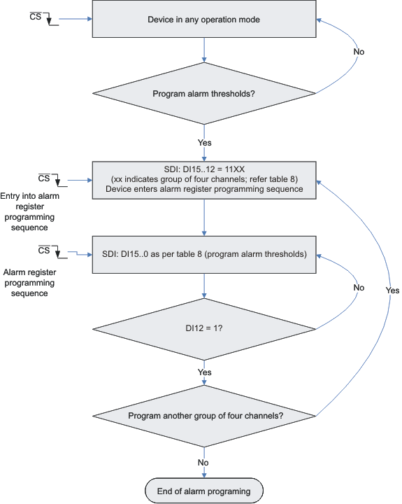
Each channel has two alarm program registers, one for setting the high alarm threshold and the other for setting the low alarm threshold. For ease of programming, two alarm programming registers per channel, corresponding to four consecutive channels, are assembled into one group (a total eight registers). There are four such groups for 16 channel devices and 3/2/1 such groups for 12/8/4 channel devices respectively. The grouping of the various channels for each device in the ADS79xx family is listed in Table 12. The details regarding programming the alarm thresholds are illustrated in the flowchart in Figure 59. Table 13 lists the details regarding the Alarm Program Register settings.
Table 12. Grouping of Alarm Program Registers
| GROUP NO. | REGISTERS | APPLICABLE FOR DEVICE |
|---|---|---|
| 0 | High and low alarm for channel 0, 1, 2, and 3 | ADS7953..50, ADS7957..54, ADS7961..58 |
| 1 | High and low alarm for channel 4, 5, 6, and 7 | ADS7953..51, ADS7957..55, ADS7961..59 |
| 2 | High and low alarm for channel 8, 9, 10, and 11 | ADS7953 and 52, ADS7957 and 56, ADS7961 and 60 |
| 3 | High and low alarm for channel 12, 13, 14, and 15 | ADS7953, ADS7957, ADS7961 |
Each alarm group requires 9 CS frames for programming their respective alarm thresholds. In the first frame the device enters the programming sequence and in each subsequent frame it programs one of the registers from the group. The device offers a feature to program less than eight registers in one programming sequence. The device exits the alarm threshold programming sequence in the next frame after it encounters the first ‘Exit Alarm Program’ bit high.

NOTE:
The device continues its operation in selected mode during programming. SDO is valid, however it is not possible to change the range or write GPIO data into the device during programming.Table 13. Alarm Program Register Settings
| BITS | RESET STATE | LOGIC STATE | FUNCTION |
|---|---|---|---|
| FRAME 1 | |||
| DI15-12 | NA | 1100 | Device enters ‘alarm programming sequence’ for group 0 |
| 1101 | Device enters ‘alarm programming sequence’ for group 1 | ||
| 1110 | Device enters ‘alarm programming sequence’ for group 2 | ||
| 1111 | Device enters ‘alarm programming sequence’ for group 3 | ||
| Note: DI15-12 = 11bb is the alarm programming request for group bb. Here ‘bb’ represents the alarm programming group number in binary format. | |||
| DI11-14 | NA | Do not care | |
| FRAME 2 AND ONWARDS | |||
| DI15-14 | NA | cc | Where “cc” represents the lower two bits of the channel number in binary format. The device programs the alarm for the channel represented by the binary number “bbcc”. “bb” is programmed in the first frame. |
| DI13 | NA | 1 | High alarm register selection |
| 0 | Low alarm register selection | ||
| DI12 | NA | 0 | Continue alarm programming sequence in next frame |
| 1 | Exit Alarm Programming in the next frame. Note: If the alarm programming sequence is not terminated using this feature then the device will remain in the alarm programming sequence state and all SDI data will be treated as alarm thresholds. | ||
| DI11-10 | NA | xx | Do not care |
| DI09-00 | All ones for high alarm register and all zeros for low alarm register | This 10-bit data represents the alarm threshold. The 10-bit alarm threshold is compared with the upper 10-bit word of the 12-bit conversion result. The device sets off an alarm when the conversion result is higher (High Alarm) or lower (Low Alarm) than this number. For 10-bit devices, all 10 bits of the conversion result are compared with the set threshold. For 8-bit devices, all 8 bits of the conversion result are compared with DI09 to DI02 and DI00, 01 are 'do not care'. | |