ZHCSIJ5C August 2018 – June 2019 ADS9224R , ADS9234R
PRODUCTION DATA.
- 1 特性
- 2 应用
- 3 说明
- 4 修订历史记录
- 5 Pin Configuration and Functions
-
6 Specifications
- 6.1 Absolute Maximum Ratings
- 6.2 ESD Ratings
- 6.3 Recommended Operating Conditions
- 6.4 Thermal Information
- 6.5 Electrical Characteristics: ADS92x4R
- 6.6 Electrical Characteristics: ADS9224R
- 6.7 Electrical Characteristics: ADS9234R
- 6.8 Timing Requirements
- 6.9 Switching Characteristics
- 6.10 Typical Characteristics: ADS9224R
- 6.11 Typical Characteristics: ADS9234R
-
7 Detailed Description
- 7.1 Overview
- 7.2 Functional Block Diagram
- 7.3 Feature Description
- 7.4 Device Functional Modes
- 7.5 READY/STROBE Output
- 7.6
Programming
- 7.6.1 Output Data Word
- 7.6.2
Data Transfer Protocols
- 7.6.2.1
Protocols for Reading From the Device
- 7.6.2.1.1 Legacy, SPI-Compatible Protocols (SPI-xy-S-SDR)
- 7.6.2.1.2 SPI-Compatible Protocols With Bus Width Options and Single Data Rate (SPI-xy-D-SDR and SPI-xy-Q-SDR)
- 7.6.2.1.3 SPI-Compatible Protocols With Bus Width Options and Double Data Rate (SPI-x1-S-DDR, SPI-x1-D-DDR, SPI-x1-Q-DDR)
- 7.6.2.1.4 Clock Re-Timer (CRT) Protocols (CRT-S-SDR, CRT-D-SDR, CRT-Q-SDR, CRT-S-DDR, CRT-D-DDR, CRT-Q-DDR)
- 7.6.2.1.5 Parallel Byte Protocols (PB-xy-AB-SDR, PB-xy-AA-SDR)
- 7.6.2.2 Device Setup
- 7.6.2.3 Protocols for Configuring the Device
- 7.6.2.1
Protocols for Reading From the Device
- 7.6.3 Reading and Writing Registers
- 7.7
Register Maps
- 7.7.1
ADS92x4R Registers
- 7.7.1.1 DEVICE_STATUS Register (Offset = 0h) [reset = 0h]
- 7.7.1.2 POWER_DOWN_CFG Register (Offset = 1h) [reset = 0h]
- 7.7.1.3 PROTOCOL_CFG Register (Offset = 2h) [reset = 0h]
- 7.7.1.4 BUS_WIDTH Register (Offset = 3h) [reset = 0h]
- 7.7.1.5 CRT_CFG Register (Offset = 4h) [reset = 0h]
- 7.7.1.6 OUTPUT_DATA_WORD_CFG Register (Offset = 5h) [reset = 0h]
- 7.7.1.7 DATA_AVG_CFG Register (Offset = 6h) [reset = 0h]
- 7.7.1.8 REFBY2_OFFSET Register (Offset = 7h) [reset = 0h]
- 7.7.1
ADS92x4R Registers
- 8 Application and Implementation
- 9 Power Supply Recommendations
- 10Layout
- 11器件和文档支持
- 12机械、封装和可订购信息
7.6.2.1.5 Parallel Byte Protocols (PB-xy-AB-SDR, PB-xy-AA-SDR)
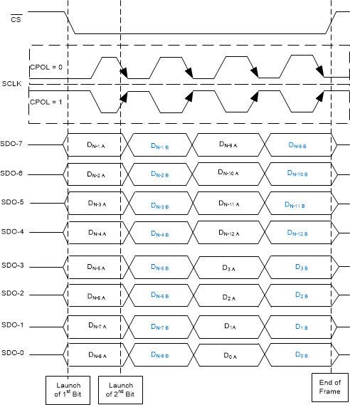
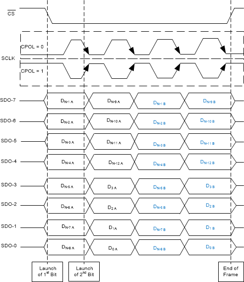
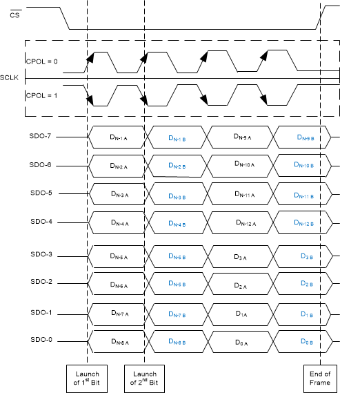
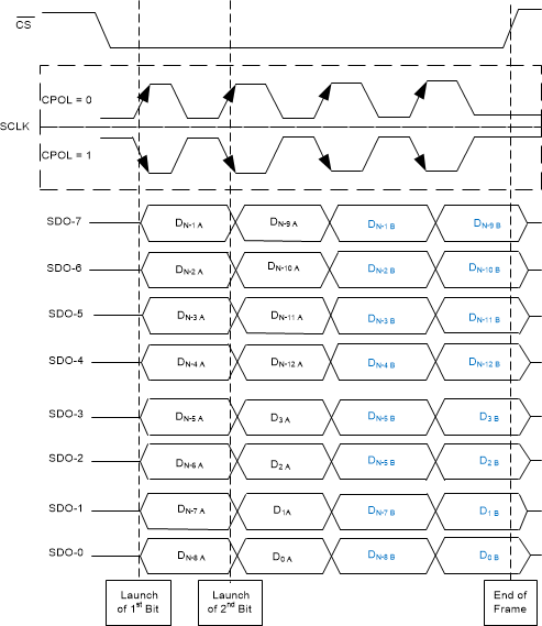
In parallel byte protocols, the device sends out data from each ADC on all SDO lines in a byte format. The device supports all combinations of CPOL and CPHA in these protocols. The format of the data byte for these protocols can be set by the PARALLEL_MODE_DATA_FORMAT bits in the OUTPUT_DATA_WORD_CFG register. The device only supports a single data rate (SDR) in parallel byte protocols. Table 7 provides the details of different parallel byte protocols to read data from the device.
Table 7. PB-xy-AB-SDR, PB-xy-AA-SDR Protocols for Reading Data
| PROTOCOL(1) | SCLK POLARITY (CPOL)(2) | SCLK PHASE (CPHA) | MSB LAUNCH EDGE | DATA FORMAT(4) | tREAD(3) | TIMING DIAGRAM |
|---|---|---|---|---|---|---|
| PB-00-AB-SDR | Low (CPOL = 0) | Rising (CPHA = 0) | CS falling | AB | [3.5 × tCLK + k] | Figure 62 |
| PB-01-AB-SDR | Low (CPOL = 0) | Falling (CPHA = 1) | 1st SCLK rising | AB | [3.5 × tCLK + k] | Figure 63 |
| PB-10-AB-SDR | High (CPOL = 1) | Falling (CPHA = 1) | CS falling | AB | [3.5 × tCLK + k] | Figure 62 |
| PB-11-AB-SDR | High (CPOL = 1) | Rising (CPHA = 0) | 1st SCLK falling | AB | [3.5 × tCLK + k] | Figure 63 |
| PB-00-AA-SDR | Low (CPOL = 0) | Rising (CPHA = 0) | CS falling | AA | [3.5 × tCLK + k] | Figure 64 |
| PB-01-AA-SDR | Low (CPOL = 0) | Falling (CPHA = 1) | 1st SCLK rising | AA | [3.5 × tCLK + k] | Figure 65 |
| PB-10-AA-SDR | High (CPOL = 1) | Falling (CPHA = 1) | CS falling | AA | [3.5 × tCLK + k] | Figure 64 |
| PB-11-AA-SDR | High (CPOL = 1) | Rising (CPHA = 0) | 1st SCLK falling | AA | [3.5 × tCLK + k] | Figure 65 |
Figure 62, Figure 63, Figure 64, and Figure 65 illustrate timing diagrams for the PB-00-AB-SDR and PB-10-AB-SDR, protocols, PB-01-AB-SDR and PB-11-AB-SDR, PB-00-AA-SDR and PB-10-AA-SDR, and PB-01-AA-SDR and PB-11-AA-SDR, respectively.
 Figure 62. PB-00-AB-SDR and PB-10-AB-SDR Protocols
  Figure 64. PB-00-AA-SDR and PB-10-AA-SDR Protocols
  Figure 63. PB-01-AB-SDR and PB-11-AB-SDR Protocols
  Figure 65. PB-01-AA-SDR and PB-11-AA-SDR Protocols