ZHCSIK6D November 2017 – June 2024 ADS8166 , ADS8167 , ADS8168
PRODUCTION DATA
- 1
- 1 特性
- 2 应用
- 3 说明
- 4 Pin Configuration and Functions
- 5 Specifications
- 6 Detailed Description
-
7 Register Maps
- 7.1
Interface and Hardware Configuration Registers
- 7.1.1 REG_ACCESS Register (address = 00h) [reset = 00h]
- 7.1.2 PD_CNTL Register (address = 04h) [reset = 00h]
- 7.1.3 SDI_CNTL Register (address = 008h) [reset = 00h]
- 7.1.4 SDO_CNTL1 Register (address = 0Ch) [reset = 00h]
- 7.1.5 SDO_CNTL2 Register (address = 0Dh) [reset = 00h]
- 7.1.6 SDO_CNTL3 Register (address = 0Eh) [reset = 00h]
- 7.1.7 SDO_CNTL4 Register (address = 0Fh) [reset = 00h]
- 7.1.8 DATA_CNTL Register (address = 10h) [reset = 00h]
- 7.1.9 PARITY_CNTL Register (address = 11h) [reset = 00h]
- 7.2 Device Calibration Registers
- 7.3 Analog Input Configuration Registers
- 7.4
Channel Sequence Configuration Registers Map
- 7.4.1 DEVICE_CFG Register (address = 1Ch) [reset = 00h]
- 7.4.2 CHANNEL_ID Register (address = 1Dh) [reset = 00h]
- 7.4.3 SEQ_START Register (address = 1Eh) [reset = 00h]
- 7.4.4 SEQ_ABORT Register (address = 1Fh) [reset = 00h]
- 7.4.5 ON_THE_FLY_CFG Register (address = 2Ah) [reset = 00h]
- 7.4.6 AUTO_SEQ_CFG1 Register (address = 80h) [reset = 00h]
- 7.4.7 AUTO_SEQ_CFG2 Register (address = 82h) [reset = 00h]
- 7.4.8
Custom Channel Sequencing Mode Registers
- 7.4.8.1 CCS_START_INDEX Register (address = 88h) [reset = 00h]
- 7.4.8.2 CCS_END_INDEX Register (address = 89h) [reset = 00h]
- 7.4.8.3 CCS_SEQ_LOOP Register (address = 8Ah) [reset = 00h]
- 7.4.8.4 CCS_CHID_INDEX_m Registers (address = 8C, 8E, 90, 92, 94, 96, 98, 9A, 9C, 9E, A0, A2, A4, A6, A8, and AAh) [reset = 00h]
- 7.4.8.5 REPEAT_INDEX_m Registers (address = 8D, 8F, 91, 93, 95, 97, 99, 9B, 9D, 9F, A1, A3, A5, A7, A9, and ABh) [reset = 00h]
- 7.5
Digital Window Comparator Configuration Registers Map
- 7.5.1 ALERT_CFG Register (address = 2Eh) [reset = 00h]
- 7.5.2 HI_TRIG_AINx[15:0] Register (address = 4Dh to 30h) [reset = 0000h]
- 7.5.3 LO_TRIG_AINx[15:0] Register (address = 71h to 54h) [reset = 0000h]
- 7.5.4 HYSTERESIS_AINx[7:0] Register (address = 4Fh to 33h) [reset = 00h]
- 7.5.5 ALERT_LO_STATUS Register (address = 78h) [reset = 00h]
- 7.5.6 ALERT_HI_STATUS Register (address = 79h) [reset = 00h]
- 7.5.7 ALERT_STATUS Register (address = 7Ah) [reset = 00h]
- 7.5.8 CURR_ALERT_LO_STATUS Register (address = 7Ch) [reset = 00h]
- 7.5.9 CURR_ALERT_HI_STATUS Register (address = 7Dh) [reset = 00h]
- 7.5.10 CURR_ALERT_STATUS Register (address = 7Eh) [reset = 00h]
- 7.1
Interface and Hardware Configuration Registers
- 8 Application and Implementation
- 9 Device and Documentation Support
- 10Revision History
- 11Mechanical, Packaging, and Orderable Information
6.3.1 Analog Multiplexer
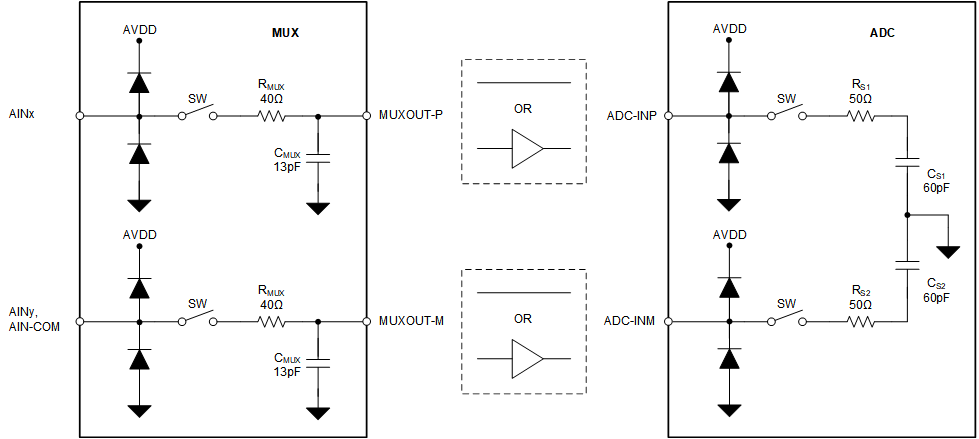
Figure 6-1 shows the small-signal equivalent circuit of the sample-and-hold circuit. Each sampling switch is represented by resistance (RS1 and RS2, typically 50Ω) in series with an ideal switch (SW). The sampling capacitors, CS1 and CS2, are typically 60pF.
The multiplexer on-resistance (RMUX), is typically a 40Ω resistor in series between the ON channel and the MUXOUT-P or MUXOUT-M pins. The multiplexer analog input typically has a 13pF on-channel capacitance (CMUX).
 Figure 6-1 Input Sampling Stage Equivalent Circuit
During the input signal acquisition phase, the ADC-INP and ADC-INM inputs are individually sampled on CS1 and CS2, respectively. During the conversion process, the device converts for the voltage difference between the two sampled values: VADC-INP – VADC-INM.
Each analog input pin has electrostatic discharge (ESD) protection diodes to AVDD and GND. Keep the analog inputs within the specified range to avoid turning the diodes on.