ZHCSIK6D November   2017  – June 2024 ADS8166 , ADS8167 , ADS8168

PRODUCTION DATA  

  1.   1
  2. 特性
  3. 应用
  4. 说明
  5. Pin Configuration and Functions
  6. Specifications
    1. 5.1 Absolute Maximum Ratings
    2. 5.2 ESD Ratings
    3. 5.3 Thermal Information
    4. 5.4 Recommended Operating Conditions
    5. 5.5 Electrical Characteristics
    6. 5.6 Timing Requirements
    7. 5.7 Switching Characteristics
    8. 5.8 Timing Diagrams
    9. 5.9 Typical Characteristics
  7. Detailed Description
    1. 6.1 Overview
    2. 6.2 Functional Block Diagram
    3. 6.3 Feature Description
      1. 6.3.1 Analog Multiplexer
        1. 6.3.1.1 Multiplexer Configurations
        2. 6.3.1.2 Multiplexer With Minimum Crosstalk
        3. 6.3.1.3 Early Switching for Direct Sensor Interface
      2. 6.3.2 Reference
      3. 6.3.3 REFby2 Buffer
      4. 6.3.4 Converter Module
        1. 6.3.4.1 Internal Oscillator
        2. 6.3.4.2 ADC Transfer Function
      5. 6.3.5 Low-Dropout Regulator (LDO)
    4. 6.4 Device Functional Modes
      1. 6.4.1 Channel Selection Using Internal Multiplexer
        1. 6.4.1.1 Manual Mode
        2. 6.4.1.2 On-The-Fly Mode
        3. 6.4.1.3 Auto Sequence Mode
        4. 6.4.1.4 Custom Channel Sequencing Mode
      2. 6.4.2 Digital Window Comparator
    5. 6.5 Programming
      1. 6.5.1 Data Transfer Protocols
        1. 6.5.1.1 Enhanced-SPI Interface
          1. 6.5.1.1.1 Protocols for Configuring the Device
          2. 6.5.1.1.2 Protocols for Reading From the Device
            1. 6.5.1.1.2.1 SPI Protocols With a Single SDO
            2. 6.5.1.1.2.2 SPI Protocols With Dual SDO
            3. 6.5.1.1.2.3 Clock Re-Timer Data Transfer
              1. 6.5.1.1.2.3.1 Output Bus Width Options
      2. 6.5.2 Register Read/Write Operation
  8. Register Maps
    1. 7.1 Interface and Hardware Configuration Registers
      1. 7.1.1 REG_ACCESS Register (address = 00h) [reset = 00h]
      2. 7.1.2 PD_CNTL Register (address = 04h) [reset = 00h]
      3. 7.1.3 SDI_CNTL Register (address = 008h) [reset = 00h]
      4. 7.1.4 SDO_CNTL1 Register (address = 0Ch) [reset = 00h]
      5. 7.1.5 SDO_CNTL2 Register (address = 0Dh) [reset = 00h]
      6. 7.1.6 SDO_CNTL3 Register (address = 0Eh) [reset = 00h]
      7. 7.1.7 SDO_CNTL4 Register (address = 0Fh) [reset = 00h]
      8. 7.1.8 DATA_CNTL Register (address = 10h) [reset = 00h]
      9. 7.1.9 PARITY_CNTL Register (address = 11h) [reset = 00h]
    2. 7.2 Device Calibration Registers
      1. 7.2.1 OFST_CAL Register (address = 18h) [reset = 00h]
      2. 7.2.2 REF_MRG1 Register (address = 19h) [reset = 00h]
      3. 7.2.3 REF_MRG2 Register (address = 1Ah) [reset = 00h]
      4. 7.2.4 REFby2_MRG Register (address = 1Bh) [reset = 00h]
    3. 7.3 Analog Input Configuration Registers
      1. 7.3.1 AIN_CFG Register (address = 24h) [reset = 00h]
      2. 7.3.2 COM_CFG Register (address = 27h) [reset = 00h]
    4. 7.4 Channel Sequence Configuration Registers Map
      1. 7.4.1 DEVICE_CFG Register (address = 1Ch) [reset = 00h]
      2. 7.4.2 CHANNEL_ID Register (address = 1Dh) [reset = 00h]
      3. 7.4.3 SEQ_START Register (address = 1Eh) [reset = 00h]
      4. 7.4.4 SEQ_ABORT Register (address = 1Fh) [reset = 00h]
      5. 7.4.5 ON_THE_FLY_CFG Register (address = 2Ah) [reset = 00h]
      6. 7.4.6 AUTO_SEQ_CFG1 Register (address = 80h) [reset = 00h]
      7. 7.4.7 AUTO_SEQ_CFG2 Register (address = 82h) [reset = 00h]
      8. 7.4.8 Custom Channel Sequencing Mode Registers
        1. 7.4.8.1 CCS_START_INDEX Register (address = 88h) [reset = 00h]
        2. 7.4.8.2 CCS_END_INDEX Register (address = 89h) [reset = 00h]
        3. 7.4.8.3 CCS_SEQ_LOOP Register (address = 8Ah) [reset = 00h]
        4. 7.4.8.4 CCS_CHID_INDEX_m Registers (address = 8C, 8E, 90, 92, 94, 96, 98, 9A, 9C, 9E, A0, A2, A4, A6, A8, and AAh) [reset = 00h]
        5. 7.4.8.5 REPEAT_INDEX_m Registers (address = 8D, 8F, 91, 93, 95, 97, 99, 9B, 9D, 9F, A1, A3, A5, A7, A9, and ABh) [reset = 00h]
    5. 7.5 Digital Window Comparator Configuration Registers Map
      1. 7.5.1  ALERT_CFG Register (address = 2Eh) [reset = 00h]
      2. 7.5.2  HI_TRIG_AINx[15:0] Register (address = 4Dh to 30h) [reset = 0000h]
      3. 7.5.3  LO_TRIG_AINx[15:0] Register (address = 71h to 54h) [reset = 0000h]
      4. 7.5.4  HYSTERESIS_AINx[7:0] Register (address = 4Fh to 33h) [reset = 00h]
      5. 7.5.5  ALERT_LO_STATUS Register (address = 78h) [reset = 00h]
      6. 7.5.6  ALERT_HI_STATUS Register (address = 79h) [reset = 00h]
      7. 7.5.7  ALERT_STATUS Register (address = 7Ah) [reset = 00h]
      8. 7.5.8  CURR_ALERT_LO_STATUS Register (address = 7Ch) [reset = 00h]
      9. 7.5.9  CURR_ALERT_HI_STATUS Register (address = 7Dh) [reset = 00h]
      10. 7.5.10 CURR_ALERT_STATUS Register (address = 7Eh) [reset = 00h]
  9. Application and Implementation
    1. 8.1 Application Information
      1. 8.1.1 Multiplexer Input Connection
    2. 8.2 Typical Applications
      1. 8.2.1 1MSPS DAQ Circuit With Lowest Distortion and Noise Performance
        1. 8.2.1.1 Design Requirements
        2. 8.2.1.2 Detailed Design Procedure
        3. 8.2.1.3 Application Curve
    3.     Power Supply Recommendations
    4. 8.3 Layout
      1. 8.3.1 Layout Guidelines
        1. 8.3.1.1 Analog Signal Path
        2. 8.3.1.2 Grounding and PCB Stack-Up
        3. 8.3.1.3 Decoupling of Power Supplies
        4. 8.3.1.4 Reference Decoupling
        5. 8.3.1.5 Reference Buffer Decoupling
        6. 8.3.1.6 Multiplexer Input Decoupling
        7. 8.3.1.7 ADC Input Decoupling
        8. 8.3.1.8 Example Schematic
      2. 8.3.2 Layout Example
  10. Device and Documentation Support
    1. 9.1 Documentation Support
      1. 9.1.1 Related Documentation
    2. 9.2 接收文档更新通知
    3. 9.3 支持资源
    4. 9.4 Trademarks
    5. 9.5 静电放电警告
    6. 9.6 术语表
  11. 10Revision History
  12. 11Mechanical, Packaging, and Orderable Information

Typical Characteristics

at AVDD = 5V, DVDD = 1.65V to 5.5V, REFIO configured as output pin, and maximum throughput (unless otherwise noted)
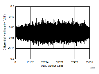
ADS8166 ADS8167 ADS8168 Typical DNL
Typical DNL = ±0.15LSB
Figure 5-5 Typical DNL
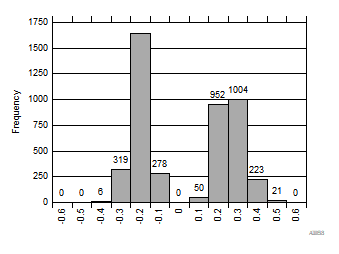
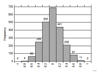
ADS8166 ADS8167 ADS8168 Typical INL Distribution (LSB)
2250 devices
Figure 5-7 Typical INL Distribution (LSB)
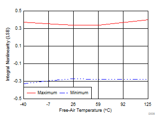
ADS8166 ADS8167 ADS8168 INL
                        vs Temperature
 
Figure 5-9 INL vs Temperature
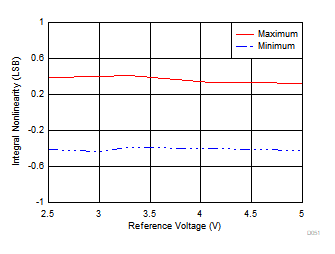
ADS8166 ADS8167 ADS8168 INL
                        vs Reference Voltage
 
Figure 5-11 INL vs Reference Voltage
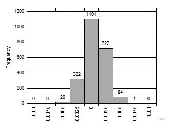
ADS8166 ADS8167 ADS8168 Typical Gain Error Distribution (%FSR)
2250 devices
Figure 5-13 Typical Gain Error Distribution (%FSR)
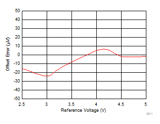
ADS8166 ADS8167 ADS8168 Offset Error vs Reference Voltage
With the appropriate REF_SEL[2:0]; see the OFST_CAL register
Figure 5-15 Offset Error vs Reference Voltage
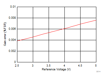
ADS8166 ADS8167 ADS8168 Gain
                        Error (ADC + REFBUF) vs Reference Voltage
EN_MARG = 0b
Figure 5-17 Gain Error (ADC + REFBUF) vs Reference Voltage
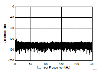
ADS8166 ADS8167 ADS8168 Typical FFT, ADS8168
fIN = 2kHz, SNR = 93.8dB, THD = –112.7dB
Figure 5-19 Typical FFT, ADS8168
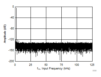
ADS8166 ADS8167 ADS8168 Typical FFT, ADS8166
fIN = 2kHz, SNR = 93.8dB, THD = –111.4dB
Figure 5-21 Typical FFT, ADS8166
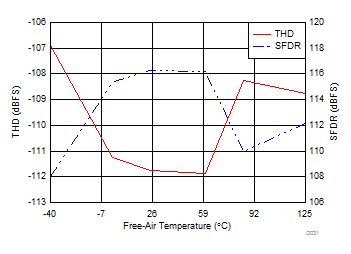
ADS8166 ADS8167 ADS8168 Distortion Performance vs Temperature
fIN = 2kHz
Figure 5-23 Distortion Performance vs Temperature
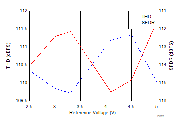
ADS8166 ADS8167 ADS8168 Distortion Performance vs Reference Voltage
fIN = 2kHz
Figure 5-25 Distortion Performance vs Reference Voltage
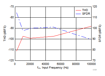
ADS8166 ADS8167 ADS8168 Distortion Performance vs Input Frequency
 
Figure 5-27 Distortion Performance vs Input Frequency
ADS8166 ADS8167 ADS8168 Analog Supply Current vs Temperature
AVDD = 5V
Figure 5-29 Analog Supply Current vs Temperature
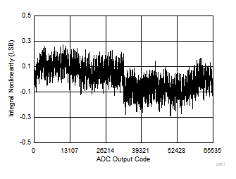
ADS8166 ADS8167 ADS8168 Typical INL
Typical INL = ±0.3LSB
Figure 5-6 Typical INL
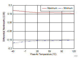
ADS8166 ADS8167 ADS8168 DNL
                        vs Temperature
 
Figure 5-8 DNL vs Temperature
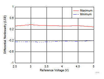
ADS8166 ADS8167 ADS8168 DNL
                        vs Reference Voltage
 
Figure 5-10 DNL vs Reference Voltage
ADS8166 ADS8167 ADS8168 Typical Offset Distribution (LSB)
2250 devices
Figure 5-12 Typical Offset Distribution (LSB)
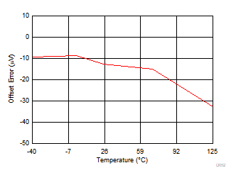
ADS8166 ADS8167 ADS8168 Offset Error vs Temperature
REF_SEL[2:0] = 000b
Figure 5-14 Offset Error vs Temperature
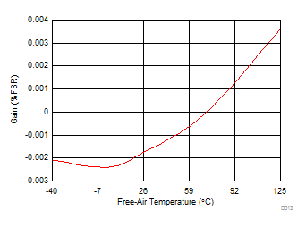
ADS8166 ADS8167 ADS8168 Gain
                        Error (ADC + REFBUF) vs Temperature
EN_MARG = 0b
 
Figure 5-16 Gain Error (ADC + REFBUF) vs Temperature
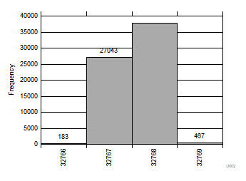
ADS8166 ADS8167 ADS8168 DC
                        Input Histogram
Standard deviation = 0.51LSB
Figure 5-18 DC Input Histogram
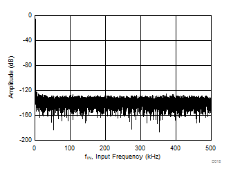
ADS8166 ADS8167 ADS8168 Typical FFT, ADS8167
fIN = 2kHz, SNR = 93.8dB, THD = –112.4dB
Figure 5-20 Typical FFT, ADS8167
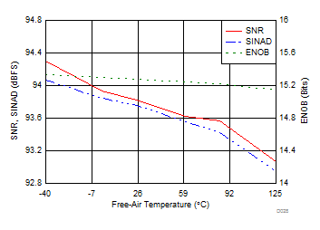
ADS8166 ADS8167 ADS8168 Noise
                        Performance vs Temperature
fIN = 2kHz
Figure 5-22 Noise Performance vs Temperature
ADS8166 ADS8167 ADS8168 Noise
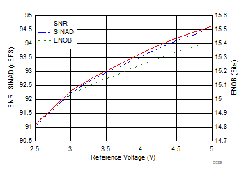
                        Performance vs Reference Voltage
fIN = 2kHz
Figure 5-24 Noise Performance vs Reference Voltage
ADS8166 ADS8167 ADS8168 Noise
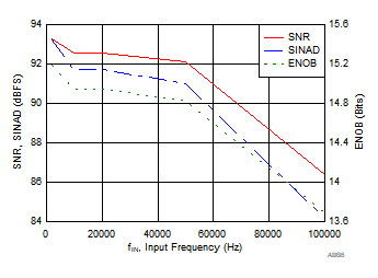
                        Performance vs Input Frequency
 
Figure 5-26 Noise Performance vs Input Frequency
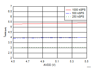
ADS8166 ADS8167 ADS8168 Analog Supply Current vs Supply Voltage
 
Figure 5-28 Analog Supply Current vs Supply Voltage