ZHCSIN4B August   2018  – June 2021 LM5146-Q1

PRODUCTION DATA  

  1. 特性
  2. 应用
  3. 说明
  4. Revision History
  5. 说明(续)
  6. Pin Configuration and Functions
    1. 6.1 Wettable Flanks
  7. Specifications
    1. 7.1 Absolute Maximum Ratings
    2. 7.2 ESD Ratings 
    3. 7.3 Recommended Operating Conditions
    4. 7.4 Thermal Information
    5. 7.5 Electrical Characteristics
    6. 7.6 Switching Characteristics
    7. 7.7 Typical Characteristics
  8. Detailed Description
    1. 8.1 Overview
    2. 8.2 Functional Block Diagram
    3. 8.3 Feature Description
      1. 8.3.1  Input Range (VIN)
      2. 8.3.2  Output Voltage Setpoint and Accuracy (FB)
      3. 8.3.3  High-Voltage Bias Supply Regulator (VCC)
      4. 8.3.4  Precision Enable (EN/UVLO)
      5. 8.3.5  Power Good Monitor (PGOOD)
      6. 8.3.6  Switching Frequency (RT, SYNCIN)
        1. 8.3.6.1 Frequency Adjust
        2. 8.3.6.2 Clock Synchronization
      7. 8.3.7  Configurable Soft Start (SS/TRK)
        1. 8.3.7.1 Tracking
      8. 8.3.8  Voltage-Mode Control (COMP)
      9. 8.3.9  Gate Drivers (LO, HO)
      10. 8.3.10 Current Sensing and Overcurrent Protection (ILIM)
      11. 8.3.11 OCP Duty Cycle Limiter
    4. 8.4 Device Functional Modes
      1. 8.4.1 Shutdown Mode
      2. 8.4.2 Standby Mode
      3. 8.4.3 Active Mode
      4. 8.4.4 Diode Emulation Mode
      5. 8.4.5 Thermal Shutdown
  9. Application and Implementation
    1. 9.1 Application Information
      1. 9.1.1 Design and Implementation
      2. 9.1.2 Power Train Components
        1. 9.1.2.1 Inductor
        2. 9.1.2.2 Output Capacitors
        3. 9.1.2.3 Input Capacitors
        4. 9.1.2.4 Power MOSFETs
      3. 9.1.3 Control Loop Compensation
      4. 9.1.4 EMI Filter Design
    2. 9.2 Typical Applications
      1. 9.2.1 Design 1 – 12-A High-Efficiency Synchronous Buck DC/DC Regulator for Automotive Applications
        1. 9.2.1.1 Design Requirements
        2. 9.2.1.2 Detailed Design Procedure
        3. 9.2.1.3 Custom Design With WEBENCH® Tools
        4. 9.2.1.4 Custom Design With Excel Quickstart Tool
        5. 9.2.1.5 Application Curves
      2. 9.2.2 Design 2 – High Density, 12-V, 8-A Rail From 48-V Automotive Battery Power
        1. 9.2.2.1 Design Requirements
        2. 9.2.2.2 Detailed Design Procedure
        3. 9.2.2.3 Application Curves
  10. 10Power Supply Recommendations
  11. 11Layout
    1. 11.1 Layout Guidelines
      1. 11.1.1 Power Stage Layout
      2. 11.1.2 Gate Drive Layout
      3. 11.1.3 PWM Controller Layout
      4. 11.1.4 Thermal Design and Layout
      5. 11.1.5 Ground Plane Design
    2. 11.2 Layout Example
  12. 12Device and Documentation Support
    1. 12.1 Device Support
      1. 12.1.1 第三方米6体育平台手机版_好二三四免责声明
      2. 12.1.2 Development Support
        1. 12.1.2.1 Custom Design With WEBENCH® Tools
    2. 12.2 Documentation Support
      1. 12.2.1 Related Documentation
        1. 12.2.1.1 PCB Layout Resources
        2. 12.2.1.2 Thermal Design Resources
    3. 12.3 接收文档更新通知
    4. 12.4 支持资源
    5. 12.5 Trademarks
    6. 12.6 Electrostatic Discharge Caution
    7. 12.7 Glossary
  13. 13Mechanical, Packaging, and Orderable Information

Clock Synchronization

Apply an external clock synchronization signal to the LM5146-Q1 to synchronize switching in both frequency and phase. Requirements for the external clock SYNC signal are:

  • Clock frequency range: 100 kHz to 1 MHz
  • Clock frequency: –20% to +50% of the free-running frequency set by RRT
  • Clock maximum voltage amplitude: 13 V
  • Clock minimum pulse width: 50 ns
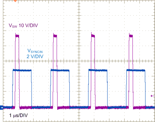
GUID-7B1C638E-CFDF-49CF-80A4-096150F3F133-low.gif Figure 8-5 Typical 400-kHz SYNCIN and SW Voltage Waveforms

Figure 8-5 shows a clock signal at 400 kHz and the corresponding SW node waveform (VIN = 48 V, VOUT = 5 V, free-running frequency = 280 kHz). The SW voltage waveform is synchronized with respect to the rising edge of SYNCIN. The rising edge of the SW voltage is phase delayed relative to SYNCIN by approximately 100 ns.