ZHCSIP2E April   2016  – October 2018 LMG3410R070 , LMG3411R070

PRODUCTION DATA.  

  1. 特性
  2. 应用
  3. 说明
    1.     Device Images
      1.      简化方框图
      2.      高于 100V/ns 时的开关性能
  4. 修订历史记录
  5. Pin Configuration and Functions
    1.     Pin Functions
  6. Specifications
    1. 6.1 Absolute Maximum Ratings
    2. 6.2 ESD Ratings
    3. 6.3 Recommended Operating Conditions
    4. 6.4 Thermal Information
    5. 6.5 Electrical Characteristics
    6. 6.6 Switching Characteristics
    7. 6.7 Typical Characteristics
  7. Parameter Measurement Information
    1. 7.1 Switching Parameters
      1. 7.1.1 Turn-on Delays
      2. 7.1.2 Turn-off Delays
      3. 7.1.3 Drain Slew Rate
      4. 7.1.4 Turn-on and Turn-off Energy
  8. Detailed Description
    1. 8.1 Overview
    2. 8.2 Functional Block Diagram
    3. 8.3 Feature Description
      1. 8.3.1 Direct-Drive GaN Architecture
      2. 8.3.2 Internal Buck-Boost DC-DC Converter
      3. 8.3.3 Internal Auxiliary LDO
      4. 8.3.4 Fault Detection
        1. 8.3.4.1 Over-current Protection
        2. 8.3.4.2 Over-Temperature Protection and UVLO
      5. 8.3.5 Drive Strength Adjustment
    4. 8.4 Device Functional Modes
      1. 8.4.1 Low-Power Mode
  9. Application and Implementation
    1. 9.1 Application Information
    2. 9.2 Typical Application
      1. 9.2.1 Design Requirements
      2. 9.2.2 Detailed Design Procedure
        1. 9.2.2.1 Slew Rate Selection
          1. 9.2.2.1.1 Startup and Slew Rate with Bootstrap High-Side Supply
        2. 9.2.2.2 Signal Level-Shifting
        3. 9.2.2.3 Buck-Boost Converter Design
      3. 9.2.3 Application Curves
    3. 9.3 Paralleling GaN Devices
    4. 9.4 Do's and Don'ts
  10. 10Power Supply Recommendations
    1. 10.1 Using an Isolated Power Supply
    2. 10.2 Using a Bootstrap Diode
      1. 10.2.1 Diode Selection
      2. 10.2.2 Managing the Bootstrap Voltage
      3. 10.2.3 Reliable Bootstrap Start-up
  11. 11Layout
    1. 11.1 Layout Guidelines
      1. 11.1.1 Power Loop Inductance
      2. 11.1.2 Signal Ground Connection
      3. 11.1.3 Bypass Capacitors
      4. 11.1.4 Switch-Node Capacitance
      5. 11.1.5 Signal Integrity
      6. 11.1.6 High-Voltage Spacing
      7. 11.1.7 Thermal Recommendations
    2. 11.2 Layout Example
  12. 12器件和文档支持
    1. 12.1 器件支持
      1. 12.1.1 第三方米6体育平台手机版_好二三四免责声明
    2. 12.2 文档支持
      1. 12.2.1 相关文档
    3. 12.3 接收文档更新通知
    4. 12.4 社区资源
    5. 12.5 商标
    6. 12.6 静电放电警告
    7. 12.7 术语表
  13. 13机械、封装和可订购信息

Managing the Bootstrap Voltage

In a synchronous buck, totem-pole PFC, or other converter where the low-side switch occasionally operates in third-quadrant mode, it is important to consider the bootstrap supply. During the dead time, the bootstrap supply charges through a path that includes the third-quadrant voltage drop of the low-side LMG341xR070. This third-quadrant drop can be large, which may over-charge the bootstrap supply in certain conditions. The VDD supply of LMG341xR070 must not exceed 18 V in bootstrap operation.
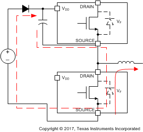
LMG3410R070 LMG3411R070 using_bootstrap_diode_snosd10.gifFigure 17. Charging Path for Bootstrap Diode

The recommended bootstrap supply connection includes a bootstrap diode and a series resistor with an optional zener as shown in Figure 18. The series resistor limits the charging current at startup and when the low-side device is operating in third-quadrant mode. This resistor must be chosen to allow sufficient current to power the LMG341xR070 at the desired operating frequency. At 100 kHz operation, a value of approximately 5.1 ohms is recommended. At higher frequencies, this resistor value should be reduced or the resistor omitted entirely to ensure sufficient supply current.
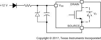
LMG3410R070 LMG3411R070 recommended_bootstrap_supply_connection_snosd10.gifFigure 18. Suggested Bootstrap Regulation Circuit

Using a series resistor with the bootstrap supply will create a charging time constant in conjunction with the bypass capacitance on the order of a microsecond. When the dead time, or third-quadrant conduction time, is much lower than this time constant, the bootstrap voltage will be well-controlled and the optional zener clamp in Figure 18 will not be necessary. If a large deadtime is needed, a 14-V zener diode can be used in parallel with the VDD bypass capacitor to prevent damaging the high-side LMG341xR070.