ZHCSIU3 September   2018 ADS1235

PRODUCTION DATA.  

  1. 特性
  2. 应用
  3. 说明
    1.     Device Images
      1.      框图
      2.      ADC 转换噪声
  4. 修订历史记录
  5. Pin Configuration and Functions
    1.     Pin Functions
  6. Specifications
    1. 6.1 Absolute Maximum Ratings
    2. 6.2 ESD Ratings
    3. 6.3 Recommended Operating Conditions
    4. 6.4 Thermal Information
    5. 6.5 Electrical Characteristics
    6. 6.6 Timing Requirements
    7. 6.7 Switching Characteristics
    8. 6.8 Typical Characteristics
  7. Parameter Measurement Information
    1. 7.1 Noise Performance
  8. Detailed Description
    1. 8.1 Overview
    2. 8.2 Functional Block Diagram
    3. 8.3 Feature Description
      1. 8.3.1 Analog Inputs
        1. 8.3.1.1 ESD Diodes
        2. 8.3.1.2 Input Multiplexer
        3. 8.3.1.3 Temperature Sensor
        4. 8.3.1.4 Inputs Open
        5. 8.3.1.5 Internal VCOM Connection
        6. 8.3.1.6 Alternate Functions
      2. 8.3.2 PGA
        1. 8.3.2.1 Input Voltage Range
        2. 8.3.2.2 PGA Bypass Mode
      3. 8.3.3 PGA Voltage Monitor
      4. 8.3.4 Reference Voltage
        1. 8.3.4.1 External Reference
        2. 8.3.4.2 AVDD – AVSS Reference (Default)
        3. 8.3.4.3 Reference Monitor
      5. 8.3.5 General-Purpose Input/Outputs (GPIOs)
      6. 8.3.6 Modulator
      7. 8.3.7 Digital Filter
        1. 8.3.7.1 Sinc Filter
          1. 8.3.7.1.1 Sinc Filter Frequency Response
        2. 8.3.7.2 FIR Filter
          1. 8.3.7.2.1 FIR Filter Frequency Response
        3. 8.3.7.3 Filter Bandwidth
        4. 8.3.7.4 50-Hz and 60-Hz Normal Mode Rejection
    4. 8.4 Device Functional Modes
      1. 8.4.1 Conversion Control
        1. 8.4.1.1 Continuous-Conversion Mode
        2. 8.4.1.2 Pulse-Conversion Mode
        3. 8.4.1.3 Conversion Latency
        4. 8.4.1.4 Start-Conversion Delay
      2. 8.4.2 Chop Mode
      3. 8.4.3 AC-Bridge Excitation Mode
      4. 8.4.4 ADC Clock Mode
      5. 8.4.5 Power-Down Mode
        1. 8.4.5.1 Hardware Power-Down
        2. 8.4.5.2 Software Power-Down
      6. 8.4.6 Reset
        1. 8.4.6.1 Power-on Reset
        2. 8.4.6.2 Reset by Pin
        3. 8.4.6.3 Reset by Command
      7. 8.4.7 Calibration
        1. 8.4.7.1 Offset and Full-Scale Calibration
          1. 8.4.7.1.1 Offset Calibration Registers
          2. 8.4.7.1.2 Full-Scale Calibration Registers
        2. 8.4.7.2 Offset Self-Calibration (SFOCAL)
        3. 8.4.7.3 Offset System-Calibration (SYOCAL)
        4. 8.4.7.4 Full-Scale Calibration (GANCAL)
        5. 8.4.7.5 Calibration Command Procedure
        6. 8.4.7.6 User Calibration Procedure
    5. 8.5 Programming
      1. 8.5.1 Serial Interface
        1. 8.5.1.1 Chip Select (CS)
        2. 8.5.1.2 Serial Clock (SCLK)
        3. 8.5.1.3 Data Input (DIN)
        4. 8.5.1.4 Data Output/Data Ready (DOUT/DRDY)
        5. 8.5.1.5 Serial Interface Auto-Reset
      2. 8.5.2 Data Ready (DRDY)
        1. 8.5.2.1 DRDY in Continuous-Conversion Mode
        2. 8.5.2.2 DRDY in Pulse-Conversion Mode
        3. 8.5.2.3 Data Ready by Software Polling
      3. 8.5.3 Conversion Data
        1. 8.5.3.1 Status byte (STATUS)
        2. 8.5.3.2 Conversion Data Format
      4. 8.5.4 CRC
      5. 8.5.5 Commands
        1. 8.5.5.1  NOP Command
        2. 8.5.5.2  RESET Command
        3. 8.5.5.3  START Command
        4. 8.5.5.4  STOP Command
        5. 8.5.5.5  RDATA Command
        6. 8.5.5.6  SYOCAL Command
        7. 8.5.5.7  GANCAL Command
        8. 8.5.5.8  SFOCAL Command
        9. 8.5.5.9  RREG Command
        10. 8.5.5.10 WREG Command
        11. 8.5.5.11 LOCK Command
        12. 8.5.5.12 UNLOCK Command
    6. 8.6 Register Map
      1. 8.6.1  Device Identification (ID) Register (address = 00h) [reset = Cxh]
        1. Table 28. ID Register Field Descriptions
      2. 8.6.2  Device Status (STATUS) Register (address = 01h) [reset = 01h]
        1. Table 29. STATUS Register Field Descriptions
      3. 8.6.3  Mode 0 (MODE0) Register (address = 02h) [reset = 24h]
        1. Table 30. MODE0 Register Field Descriptions
      4. 8.6.4  Mode 1 (MODE1) Register (address = 03h) [reset = 01h]
        1. Table 31. MODE1 Register Field Descriptions
      5. 8.6.5  Mode 2 (MODE2) Register (address = 04h) [reset = 00h]
        1. Table 32. MODE2 Register Field Descriptions
      6. 8.6.6  Mode 3 (MODE3) Register (address = 05h) [reset = 00h]
        1. Table 33. MODE3 Register Field Descriptions
      7. 8.6.7  Reference Configuration (REF) Register (address = 06h) [reset = 05h]
        1. Table 34. REF Register Field Descriptions
      8. 8.6.8  Offset Calibration (OFCALx) Registers (address = 07h, 08h, 09h) [reset = 00h, 00h, 00h]
        1. Table 35. OFCAL0, OFCAL1, OFCAL2 Registers Field Description
      9. 8.6.9  Full-Scale Calibration (FSCALx) Registers (address = 0Ah, 0Bh, 0Ch) [reset = 00h, 00h, 40h]
        1. Table 36. FSCAL0, FSCAL1, FSCAL2 Registers Field Description
      10. 8.6.10 Reserved (RESERVED) Register (address = 0Dh) [reset = FFh]
        1. Table 37. RESERVED Register Field Descriptions
      11. 8.6.11 Reserved (RESERVED) Register (address = 0Eh) [reset = 00h]
        1. Table 38. RESERVED Register Field Descriptions
      12. 8.6.12 Reserved (RESERVED) Register (address = 0Fh) [reset = 00h]
        1. Table 39. RESERVED Register Field Descriptions
      13. 8.6.13 PGA Configuration (PGA) Register (address = 10h) [reset = 00h]
        1. Table 40. PGA Register Field Descriptions
      14. 8.6.14 Input Multiplexer (INPMUX) Register (address = 11h) [reset = FFh]
        1. Table 41. INPMUX Register Field Descriptions
  9. Application and Implementation
    1. 9.1 Application Information
      1. 9.1.1 Input Range
      2. 9.1.2 Input Overload
      3. 9.1.3 Unused Inputs and Outputs
      4. 9.1.4 Multiplexed 2-Bridge Input Example
      5. 9.1.5 AC-Bridge Excitation Example
      6. 9.1.6 Serial Interface and Digital Connections
    2. 9.2 Typical Application
      1. 9.2.1 Design Requirements
      2. 9.2.2 Detailed Design Procedure
      3. 9.2.3 Application Curves
    3. 9.3 Initialization Setup
  10. 10Power Supply Recommendations
    1. 10.1 Power-Supply Decoupling
    2. 10.2 Analog Power-Supply Clamp
    3. 10.3 Power-Supply Sequencing
  11. 11Layout
    1. 11.1 Layout Guidelines
    2. 11.2 Layout Example
  12. 12器件和文档支持
    1. 12.1 文档支持
      1. 12.1.1 相关文档
    2. 12.2 接收文档更新通知
    3. 12.3 社区资源
    4. 12.4 商标
    5. 12.5 静电放电警告
    6. 12.6 术语表
  13. 13机械、封装和可订购信息

Typical Characteristics

at TA = 25°C, AVDD = 5 V, AVSS = 0 V, DVDD = 3.3 V, VREF = 5 V, data rate = 20 SPS, fCLK = 7.3728 MHz and gain = 128 (unless otherwise noted)
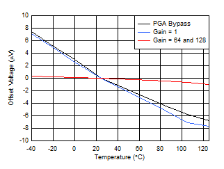
ADS1235 D009_SBAS824.gif
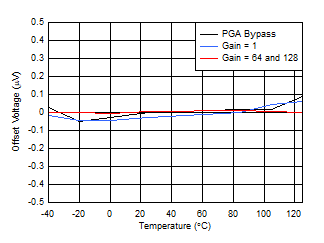
After calibration, shorted input
Figure 9. Offset Voltage vs Temperature
ADS1235 D012_SBAS824.gif
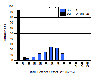
Shorted input, 30 units
Figure 11. Offset Voltage Drift Distribution
ADS1235 D001_SBAS824.gif
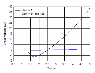
After calibration
Figure 13. Offset Voltage vs Reference Voltage
ADS1235 D013_SBAS824.gif
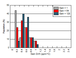
30 units
Figure 15. Gain Drift Distribution
ADS1235 D003_SBAS824.gif
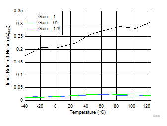
20 SPS, Sinc4 mode
Figure 17. Noise vs Temperature
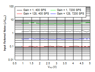
ADS1235 D006_SBAS824.gif
Figure 19. Noise vs Reference Voltage
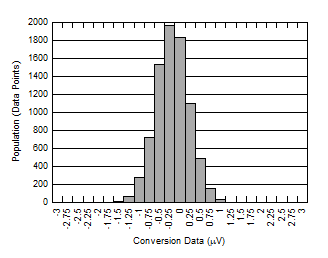
ADS1235 D031_SBAS824.gif
7200 SPS, Gain = 128, 8192 data points, shorted inputs
Figure 21. Conversion Data Histogram
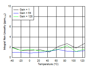
ADS1235 D007_SBAS824.gif
Figure 23. Integral Non-Linearity vs Temperature
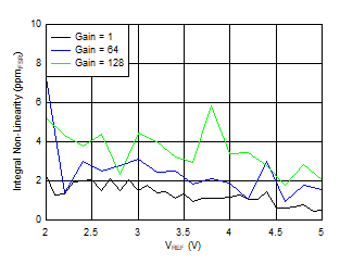
ADS1235 D008_SBAS824.gif
Figure 25. Integral Non-Linearity vs Reference Voltage
ADS1235 D112_SBAS824.gif
Chop Mode, Gain = 128
Figure 27. Differential Input Current
ADS1235 D113_SBAS824.gif
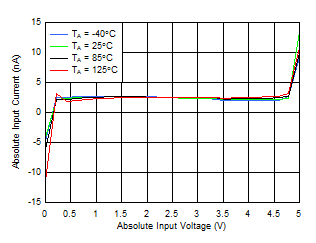
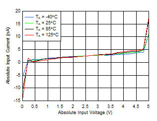
Gain = 128
Figure 29. Absolute Input Current
ADS1235 D024_SBAS760.gif
VREFN = AVSS
Figure 31. Reference Input Current vs Reference Voltage
ADS1235 D016_SBAS760.gif
30 units
Figure 33. Internal Oscillator Frequency vs Temperature
ADS1235 D026_SBAS824.gif
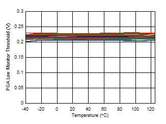
30 units
Figure 35. PGA Low Monitor Threshold vs Temperature
ADS1235 D034_SBAS760.gif
Figure 37. CMRR and PSRR vs Temperature
ADS1235 D010_SBAS824.gif
Chop mode, after calibration, shorted input
Figure 10. Offset Voltage vs Temperature
ADS1235 D011_SBAS824.gif
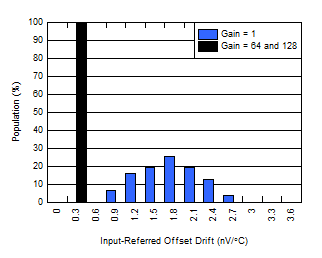
Chop mode, shorted input, 30 units
Figure 12. Offset Voltage Drift Distribution
ADS1235 D014_SBAS824.gif
After calibration
Figure 14. Gain Error vs Temperature
ADS1235 D002_SBAS824.gif
After calibration
Figure 16. Gain vs Reference Voltage
ADS1235 D004_SBAS824.gif
7200 SPS, Sinc1 mode
Figure 18. Noise vs Temperature
ADS1235 D029_SBAS824.gif
20 SPS, Gain = 128, 256 data points, shorted inputs
Figure 20. Conversion Data Histogram
ADS1235 D033_SBAS824.gif
Figure 22. Integral Non-Linearity vs VIN
ADS1235 D015_SBAS824.gif
30 Units
Figure 24. Integral Non-Linearity Distribution
ADS1235 D110_SBAS824.gif
Gain = 128
Figure 26. Differential Input Current
ADS1235 D111_SBAS824.gif
PGA Bypass (gain = 1)
Figure 28. Differential Input Current
ADS1235 D114_SBAS824.gif
Chop Mode, Gain = 128
Figure 30. Absolute Input Current
ADS1235 D017_SBAS760.gif
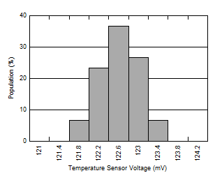
30 units
Figure 32. Temperature Sensor Voltage Histogram
ADS1235 D027_SBAS760.gif
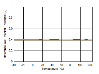
30 units
Figure 34. Reference Low Monitor Threshold vs Temperature
ADS1235 D025_SBAS824.gif
30 units
Figure 36. PGA High Monitor Threshold vs Temperature
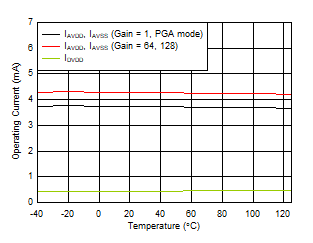
ADS1235 D018_SBAS824.gif
Figure 38. Operating Current vs Temperature