ZHCSIU6F September 2018 – June 2021 TPS2663
PRODUCTION DATA
- 1 特性
- 2 应用
- 3 说明
- 4 Revision History
- 5 Device Comparison Table
- 6 Pin Configuration and Functions
- 7 Specifications
- 8 Parameter Measurement Information
-
9 Detailed Description
- 9.1 Overview
- 9.2 Functional Block Diagram
- 9.3
Feature Description
- 9.3.1 Hot Plug-In and In-Rush Current Control
- 9.3.2 PGOOD and PGTH
- 9.3.3 Undervoltage Lockout (UVLO)
- 9.3.4 Overvoltage Protection (OVP)
- 9.3.5 Input Reverse Polarity Protection (B_GATE, DRV)
- 9.3.6 Reverse Current Protection
- 9.3.7 Overload and Short Circuit Protection
- 9.3.8 Output Power Limiting, PLIM (TPS26632, TPS26633, TPS26635 and TPS26636 Only)
- 9.3.9 Current Monitoring Output (IMON)
- 9.3.10 FAULT Response ( FLT)
- 9.3.11 IN_SYS, IN, OUT and GND Pins
- 9.3.12 Thermal Shutdown
- 9.3.13 Low Current Shutdown Control (SHDN)
- 9.4 Device Functional Modes
-
10Application and Implementation
- 10.1 Application Information
- 10.2
Typical Application: Power Path Protection in a PLC System
- 10.2.1 Design Requirements
- 10.2.2 Detailed Design Procedure
- 10.2.3 Application Curves
- 10.3 System Examples
- 10.4 Do's and Don'ts
- 11Power Supply Recommendations
- 12Layout
- 13Device and Documentation Support
- 14Mechanical, Packaging, and Orderable Information
6 Pin Configuration and Functions
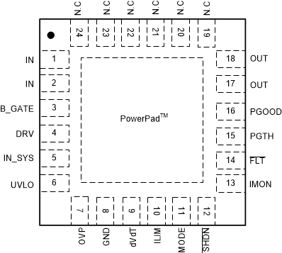
 Figure 6-1 TPS26630, TPS26631 RGE Package24-Pin VQFNTop View
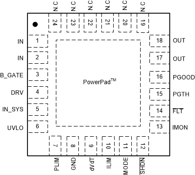
 Figure 6-3 TPS26632, TPS26633, TPS26635 RGE
Package24-Pin VQFNTop View
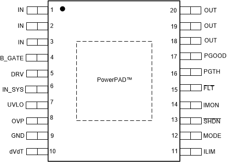
 Figure 6-2 TPS26631 PWP Package20-Pin HTSSOPTop View
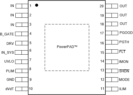
 Figure 6-4 TPS26633, TPS26636 PWP Package20-Pin HTSSOPTop View
Table 6-1 Pin Configuration and Functions
| PIN | TYPE | DESCRIPTION | ||
|---|---|---|---|---|
| NAME | TPS26630, TPS26631, TPS26632, TPS26633, TPS26635, TPS26636 | |||
| VQFN | HTSSOP | |||
| IN | 1 | 1 | P | Power input. Connects to the DRAIN of the internal FET |
| 2 | 2 | |||
| — | 3 | |||
| B_GATE | 3 | 4 | O | Blocking FET gate driver output. Connect B_GATE to GATE of the external NFET. If external FET is not used then leave B_GATE pin floating. See the Input Reverse Polarity Protection (B_GATE, DRV) section. |
| DRV | 4 | 5 | O | Blocking FET fast pull down switch drive. Connect DRV to the GATE of external pull down switch. Leave this pin floating if external N-FET is not used. |
| IN_SYS | 5 | 6 | P | Power input and supply voltage of the device. When an external Blocking FET is used then connect IN_SYS to source of the FET. Short IN_SYS to IN in case blocking FET is not used. |
| UVLO | 6 | 7 | I | Input for setting the programmable undervoltage lockout threshold. An undervoltage event turns off the internal FET and asserts FLT to indicate the power-failure. Connect UVLO pin to GND pin to select the internal default threshold. |
| OVP | 7 | 8 | I | Input for setting the programmable overvoltage protection threshold (For TPS26630 and TPS26631 Only). An overvoltage event turns off the internal FET and asserts FLT to indicate the overvoltage fault. Connect OVP pin to GND pin externally to select the internal default threshold. |
| PLIM | 7 | 8 | I | Input for setting the programmable output power limiting threshold (For TPS26632, TPS26633, TPS26635 and TPS26636 Only). Connect a resistor across PLIM to GND to set the output power limit. Connect PLIM to GND if PLIM feature is not used. See the tput power limit. Connect PLIM to GND if PLIM feature is not used. See the Output Power Limiting, PLIM (TPS26632, TPS26633, TPS26635 and TPS26636 Only) section. |
| GND | 8 | 9 | — | Connect GND to system ground |
| dVdT | 9 | 10 | I/O | A capacitor from this pin to GND sets output voltage slew rate. See the Hot Plug-In and In-Rush Current Control section. |
| ILIM | 10 | 11 | I/O | A resistor from this pin to GND sets the overload and short-circuit current limit. See the Overload and Short Circuit Protection section. |
| MODE | 11 | 12 | I | Mode selection pin for overload fault response. See the Device Functional Modes section. |
| SHDN | 12 | 13 | I | Shutdown pin. Pulling SHDN low makes the device to enter into low power shutdown mode. Cycling SHDN pin voltage resets the device that has latched off due to a fault condition. |
| IMON | 13 | 14 | O | Analog current monitor output. This pin sources a scaled down ratio of current through the internal FET. A resistor from this pin to GND converts current to proportional voltage. If unused, leave it floating. |
| FLT | 14 | 15 | O | Fault event indicator. It is an open drain output. If unused, leave floating or connect to GND. |
| PGTH | 15 | 16 | I | PGOOD comparator input. |
| PGOOD | 16 | 17 | O | Active High. A high indicates PGTH has crossed the V(PGTHR) threshold and the internal FET is enhanced. PGOOD goes low when V(PGTH) hits V(PGTHF) threshold. If PGOOD is unused then connect to GND or leave it floating. |
| OUT | 17 | 18 | P | Power output of the device |
| 18 | 19 | |||
| — | 20 | |||
| N. C | 19 | — | — | No Connect |
| 20 | ||||
| 21 | ||||
| 22 | ||||
| 23 | ||||
| 24 | ||||
| PowerPadTM | — | — | — | Connect PowerPad to GND plane for heat sinking. Do not use PowerPad as the only electrical connection to GND. |