ZHCSIZ5E October 2018 – June 2021 IWR6443 , IWR6843
PRODUCTION DATA
- 1 特性
- 2 应用
- 3 说明
- 4 功能方框图
- 5 Revision History
- 6 Device Comparison
- 7 Terminal Configuration and Functions
-
8 Specifications
- 8.1 Absolute Maximum Ratings
- 8.2 ESD Ratings
- 8.3 Power-On Hours (POH)
- 8.4 Recommended Operating Conditions
- 8.5 Power Supply Specifications
- 8.6 Power Consumption Summary
- 8.7 RF Specification
- 8.8 CPU Specifications
- 8.9 Thermal Resistance Characteristics for FCBGA Package [ABL0161]
- 8.10
Timing and Switching Characteristics
- 8.10.1 Power Supply Sequencing and Reset Timing
- 8.10.2 Input Clocks and Oscillators
- 8.10.3
Multibuffered / Standard Serial Peripheral Interface (MibSPI)
- 8.10.3.1 Peripheral Description
- 8.10.3.2
MibSPI Transmit and Receive RAM Organization
- 8.10.3.2.1 SPI Timing Conditions
- 8.10.3.2.2 SPI Master Mode Switching Parameters (CLOCK PHASE = 0, SPICLK = output, SPISIMO = output, and SPISOMI = input) (1) (1) (1)
- 8.10.3.2.3 SPI Master Mode Switching Parameters (CLOCK PHASE = 1, SPICLK = output, SPISIMO = output, and SPISOMI = input) (1) (1) (1)
- 8.10.3.3 SPI Slave Mode I/O Timings
- 8.10.3.4 Typical Interface Protocol Diagram (Slave Mode)
- 8.10.4 LVDS Interface Configuration
- 8.10.5 General-Purpose Input/Output
- 8.10.6 Controller Area Network - Flexible Data-rate (CAN-FD)
- 8.10.7 Serial Communication Interface (SCI)
- 8.10.8 Inter-Integrated Circuit Interface (I2C)
- 8.10.9 Quad Serial Peripheral Interface (QSPI)
- 8.10.10 ETM Trace Interface
- 8.10.11 Data Modification Module (DMM)
- 8.10.12 JTAG Interface
- 9 Detailed Description
- 10Monitoring and Diagnostics
- 11Applications, Implementation, and Layout
- 12Device and Documentation Support
- 13Mechanical, Packaging, and Orderable Information
9.3.1.1 Clock Subsystem
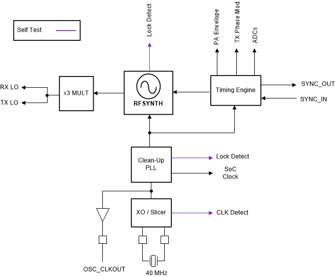
The IWR6843 clock subsystem generates 60 to 64 GHz from an input reference of 40-MHz crystal. It has a built-in oscillator circuit followed by a clean-up PLL and a RF synthesizer circuit. The output of the RF synthesizer is then processed by an X3 multiplier to create the required frequency in the 60 to 64 GHz spectrum. The RF synthesizer output is modulated by the timing engine block to create the required waveforms for effective sensor operation.
The clean-up PLL also provides a reference clock for the host processor after system wakeup.
The clock subsystem also has built-in mechanisms for detecting the presence of a crystal and monitoring the quality of the generated clock.
Figure 9-2 describes the clock subsystem.
 Figure 9-2 Clock Subsystem