ZHCSIZ6C October   2018  – June 2019 ADS125H02

PRODUCTION DATA.  

  1. 特性
  2. 应用
  3. 说明
    1.     功能方框图
  4. 修订历史记录
  5. Device Comparison Table
  6. Pin Configuration and Functions
    1.     Pin Functions
  7. Specifications
    1. 7.1 Absolute Maximum Ratings
    2. 7.2 ESD Ratings
    3. 7.3 Recommended Operating Conditions
    4. 7.4 Thermal Information
    5. 7.5 Electrical Characteristics
    6. 7.6 Timing Requirements
    7. 7.7 Switching Characteristics
    8. 7.8 Typical Characteristics
  8. Parameter Measurement Information
    1. 8.1 Noise Performance
  9. Detailed Description
    1. 9.1 Overview
    2. 9.2 Functional Block Diagram
    3. 9.3 Feature Description
      1. 9.3.1 Input Range
      2. 9.3.2 Analog Inputs
        1. 9.3.2.1 ESD Diodes
        2. 9.3.2.2 Input Multiplexer
          1. 9.3.2.2.1 Analog Inputs (AIN0, AIN1, AINCOM)
          2. 9.3.2.2.2 High-Voltage Power Supply Readback
          3. 9.3.2.2.3 Internal VCOM Connection (Default)
          4. 9.3.2.2.4 Temperature Sensor
      3. 9.3.3 Programmable Gain Amplifier (PGA)
        1. 9.3.3.1 PGA Operating Range
        2. 9.3.3.2 PGA Monitor
      4. 9.3.4 Reference Voltage
        1. 9.3.4.1 Internal Reference
        2. 9.3.4.2 External Reference
        3. 9.3.4.3 AVDD Power-Supply Reference
        4. 9.3.4.4 Reference Monitor
      5. 9.3.5 Current Sources (IDAC1 and IDAC2)
      6. 9.3.6 General-Purpose Inputs and Outputs (GPIOs)
      7. 9.3.7 ADC Modulator
      8. 9.3.8 Digital Filter
        1. 9.3.8.1 Sinc Filter Mode
          1. 9.3.8.1.1 Sinc Filter Frequency Response
        2. 9.3.8.2 FIR Filter
        3. 9.3.8.3 50-Hz and 60-Hz Normal Mode Rejection
    4. 9.4 Device Functional Modes
      1. 9.4.1 Conversion Control
        1. 9.4.1.1 Continuous-Conversion Mode
        2. 9.4.1.2 Pulse-Conversion Mode
        3. 9.4.1.3 Conversion Latency
        4. 9.4.1.4 Start-Conversion Delay
      2. 9.4.2 Auto-Zero Mode
      3. 9.4.3 Clock Mode
      4. 9.4.4 Reset
        1. 9.4.4.1 Power-On Reset
        2. 9.4.4.2 Reset by Pin
        3. 9.4.4.3 Reset by Command
      5. 9.4.5 Calibration
        1. 9.4.5.1 Offset and Full-Scale Calibration
          1. 9.4.5.1.1 Offset Calibration Registers
          2. 9.4.5.1.2 Full-Scale Calibration Registers
        2. 9.4.5.2 Offset Calibration (OFSCAL)
        3. 9.4.5.3 Full-Scale Calibration (GANCAL)
        4. 9.4.5.4 Calibration Command Procedure
        5. 9.4.5.5 User Calibration Procedure
    5. 9.5 Programming
      1. 9.5.1 Serial Interface
        1. 9.5.1.1 Chip-Select Pins (CS1 and CS2)
        2. 9.5.1.2 Serial Clock (SCLK)
        3. 9.5.1.3 Data Input (DIN)
        4. 9.5.1.4 Data Output/Data Ready (DOUT/DRDY)
      2. 9.5.2 Data Ready (DRDY)
        1. 9.5.2.1 DRDY in Continuous-Conversion Mode
        2. 9.5.2.2 DRDY in Pulse-Conversion Mode
        3. 9.5.2.3 Data Ready by Software Polling
      3. 9.5.3 Conversion Data
        1. 9.5.3.1 Status Byte (STATUS0)
        2. 9.5.3.2 Conversion Data Format
      4. 9.5.4 Cyclic Redundancy Check (CRC)
      5. 9.5.5 Commands
        1. 9.5.5.1  General Command Format
        2. 9.5.5.2  NOP Command
        3. 9.5.5.3  RESET Command
        4. 9.5.5.4  START Command
        5. 9.5.5.5  STOP Command
        6. 9.5.5.6  RDATA Command
        7. 9.5.5.7  OFSCAL Command
        8. 9.5.5.8  GANCAL Command
        9. 9.5.5.9  RREG Command
        10. 9.5.5.10 WREG Command
        11. 9.5.5.11 LOCK Command
        12. 9.5.5.12 UNLOCK Command
    6. 9.6 Register Map
      1. 9.6.1  Device Identification (ID) Register (address = 00h) [reset = 6xh]
        1. Table 30. ID Register Field Descriptions
      2. 9.6.2  Main Status (STATUS0) Register (address = 01h) [reset = 01h]
        1. Table 31. STATUS0 Register Field Descriptions
      3. 9.6.3  Mode 0 (MODE0) Register (address = 02h) [reset = 24h]
        1. Table 32. MODE0 Register Field Descriptions
      4. 9.6.4  Mode 1 (MODE1) Register (address = 03h) [reset = 01h]
        1. Table 33. MODE1 Register Field Descriptions
      5. 9.6.5  Mode 2 (MODE2) Register (address = 04h) [reset = 00h]
        1. Table 34. MODE2 Register Field Descriptions
      6. 9.6.6  Mode 3 (MODE3) Register (address = 05h) [reset = 00h]
        1. Table 35. MODE3 Register Field Descriptions
      7. 9.6.7  Reference Configuration (REF) Register (address = 06h) [reset = 05h]
        1. Table 36. REF Register Field Descriptions
      8. 9.6.8  Offset Calibration (OFCALx) Registers (address = 07h, 08h, 09h) [reset = 00h, 00h, 00h]
        1. Table 37. OFCAL0, OFCAL1, OFCAL2 Registers Field Description
      9. 9.6.9  Full-Scale Calibration (FSCALx) Registers (address = 0Ah, 0Bh, 0Ch) [reset = 00h, 00h, 40h]
        1. Table 38. FSCAL0, FSCAL1, FSCAL2 Registers Field Description
      10. 9.6.10 Current Source Multiplexer (I_MUX) Register (address = 0Dh) [reset = FFh]
        1. Table 39. I_MUX Register Field Descriptions
      11. 9.6.11 Current Source Magnitude (I_MAG) Register (address = 0Eh) [reset = 00h]
        1. Table 40. I_MAG Register Field Descriptions
      12. 9.6.12 Reserved (RESERVED) Register (address = 0Fh) [reset = 00h]
        1. Table 41. RESERVED Register Field Descriptions
      13. 9.6.13 MODE4 (MODE4) Register (address = 10h) [reset = 50h]
        1. Table 42. MODE4 Register Field Descriptions
      14. 9.6.14 PGA Alarm (STATUS1) Register (address = 11h) [reset = xxh]
        1. Table 43. STATUS1 Register Field Descriptions
      15. 9.6.15 Status 2 (STATUS2) Register (address = 12h) [reset = 0xh]
        1. Table 44. STATUS2 Register Field Descriptions
  10. 10Application and Implementation
    1. 10.1 Application Information
      1. 10.1.1 Input Range
      2. 10.1.2 Input Overload
        1. 10.1.2.1 Input Signal Rate of Change (dV/dt)
      3. 10.1.3 Unused Inputs and Outputs
    2. 10.2 Typical Applications
      1. 10.2.1 ±10-V Analog Input Module
        1. 10.2.1.1 Design Requirements
        2. 10.2.1.2 Detailed Design Procedure
        3. 10.2.1.3 Application Curves
      2. 10.2.2 Thermocouple Input With High Common-Mode Voltage
    3. 10.3 Initialization Setup
  11. 11Power Supply Recommendations
    1. 11.1 Power-Supply Decoupling
    2. 11.2 Analog Power-Supply Clamp
    3. 11.3 Power-Supply Sequencing
    4. 11.4 5-V to ±15-V DC-DC Converter
  12. 12Layout
    1. 12.1 Layout Guidelines
    2. 12.2 Layout Example
  13. 13器件和文档支持
    1. 13.1 文档支持
      1. 13.1.1 相关文档
    2. 13.2 接收文档更新通知
    3. 13.3 社区资源
    4. 13.4 商标
    5. 13.5 静电放电警告
    6. 13.6 Glossary
  14. 14机械、封装和可订购信息

Typical Characteristics

at TA = 25°C, HV_AVDD = 15 V, HV_AVSS = –15 V, AVDD = 5 V, DVDD = 3.3 V, VREF = 2.5 V, fCLK = 7.3728 MHz, data rate = 20 SPS, and gain = 1 (unless otherwise noted)
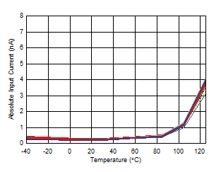
ADS125H02 D042_SBAS790.gif
V(AINx) = 0 V
Figure 6. Absolute Analog Input Current vs Temperature
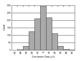
ADS125H02 D018_SBAS790.gif
Gain = 0.1875, data rate = 1200 SPS, sinc1 filter, calibrated offset,
en = 13.6 µVRMS
Figure 8. Noise Histogram
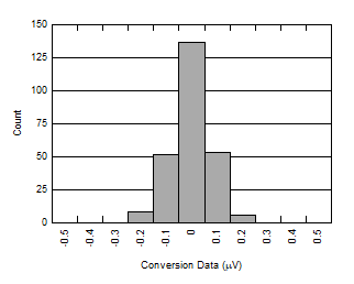
ADS125H02 D020_SBAS790.gif
Gain = 32, data rate = 20 SPS, FIR filter, calibrated offset,
en = 0.076 µVRMS
Figure 10. Noise Histogram
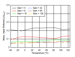
ADS125H02 D025_SBAS790.gif
Gain = 4 to 128, data rate = 20 SPS
Figure 12. Noise vs Temperature
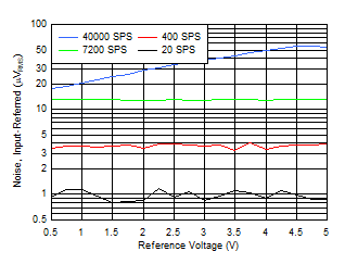
ADS125H02 D016_SBAS790.gif
Gain = 1
Figure 14. Noise vs Reference Voltage
ADS125H02 D026_SBAS790.gif
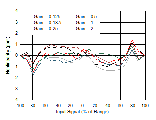
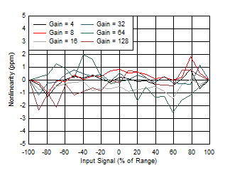
Figure 16. Nonlinearity vs Input Signal
ADS125H02 D023_SBAS790.gif
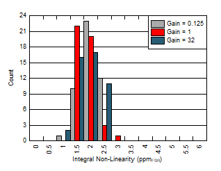
Figure 18. Integral Nonlinearity Distribution
ADS125H02 D022_SBAS790.gif
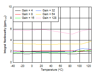
Figure 20. Integral Nonlinearity vs Temperature
ADS125H02 D010_SBAS790.gif
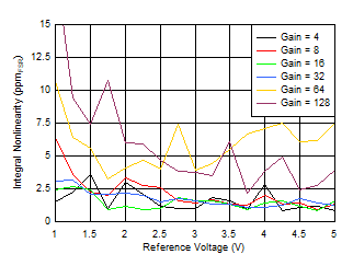
Input range limited to: ±4 V / Gain when VREF > 4 V
Figure 22. Integral Nonlinearity vs Reference Voltage
ADS125H02 D036_SBAS790.gif
Gain = 1
Figure 24. Offset Voltage Drift Distribution
ADS125H02 D039_SBAS790.gif
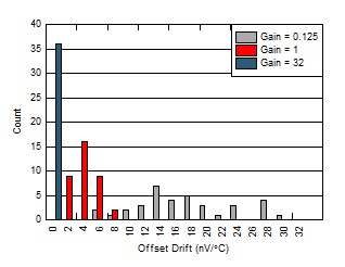
Auto-zero mode
Figure 26. Offset Voltage Drift Distribution
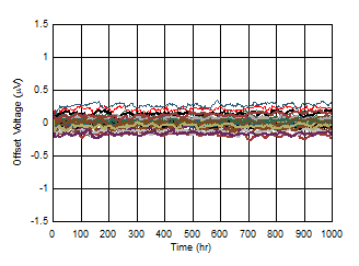
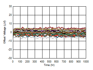
ADS125H02 D053_SBAS790.gif
32 units, gain = 32, after calibration
Figure 28. Offset Voltage Long-Term Drift
ADS125H02 D014_SBAS790.gif
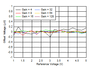
Gain = 4 to 128, after calibration
Figure 30. Offset Voltage vs Reference Voltage
ADS125H02 D038_SBAS790.gif
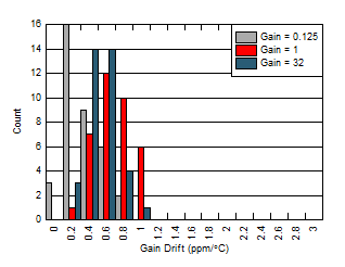
Figure 32. Gain Drift Distribution
ADS125H02 D029_SBAS790.gif
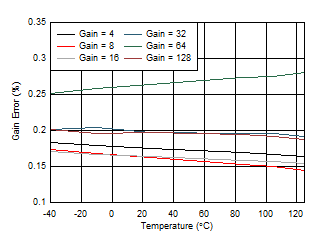
Gain = 4 to 128
Figure 34. Gain Error vs Temperature
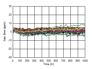
ADS125H02 D051_SBAS790.gif
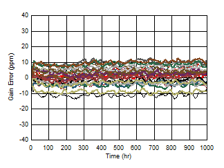
32 units, gain = 32, after calibration
Figure 36. Gain Long-Term Drift
ADS125H02 D012_SBAS790.gif
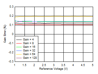
Measurement input range limited to: ±4 V / Gain when VREF > 4 V
Figure 38. Gain Error vs Reference Voltage
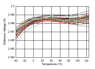
ADS125H02 D006_SBAS790.gif
Figure 40. Internal Reference Voltage vs Temperature
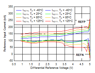
ADS125H02 D024_SBAS760.gif
Figure 42. Reference Input Current vs Reference Voltage
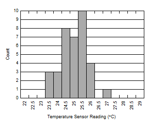
ADS125H02 D041_SBAS790.gif
TA = 25°C
Figure 44. Temperature Sensor Reading Distribution
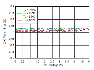
ADS125H02 D023_SBAS760.gif
IDAC = 250 µA
Figure 46. IDAC Match Error vs IDAC Voltage
ADS125H02 D049_SBAS790.gif
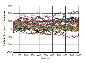
32 units, normalized data
Figure 48. Oscillator Frequency Long-Term Drift
ADS125H02 D032_SBAS790.gif
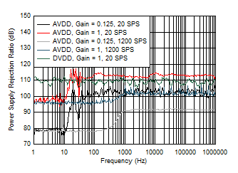
AVDD and DVDD
Figure 50. PSRR vs Frequency
ADS125H02 D043_SBAS790.gif
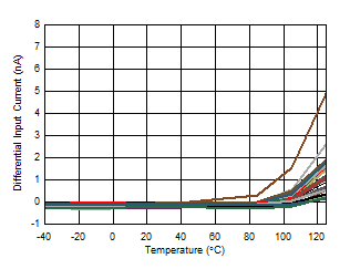
VIN = 2.5 V
Figure 7. Differential Analog Input Current vs Temperature
ADS125H02 D019_SBAS790.gif
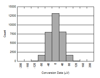
Gain = 1, data rate = 40000 SPS, calibrated offset,
en = 37 µVRMS
Figure 9. Noise Histogram
ADS125H02 D024_SBAS790.gif
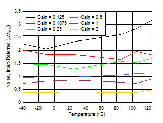
Gain = 0.125 to 2, data rate = 20 SPS
Figure 11. Noise vs Temperature
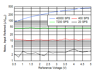
ADS125H02 D015_SBAS790.gif
Gain = 0.125
Figure 13. Noise vs Reference Voltage
ADS125H02 D017_SBAS790.gif
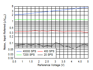
Gain = 16
Figure 15. Noise vs Reference Voltage
ADS125H02 D027_SBAS790.gif
Figure 17. Nonlinearity vs Input Signal
ADS125H02 D021_SBAS790.gif
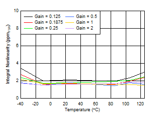
Figure 19. Integral Nonlinearity vs Temperature
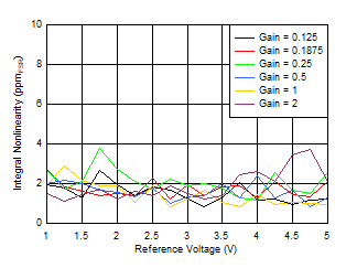
ADS125H02 D009_SBAS790.gif
Input range limited to: ±4 V / Gain when VREF > 4 V
Figure 21. Integral Nonlinearity vs Reference Voltage
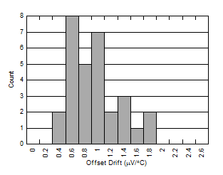
ADS125H02 D035_SBAS790.gif
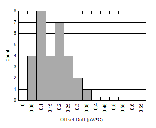
Gain = 0.125
Figure 23. Offset Voltage Drift Distribution
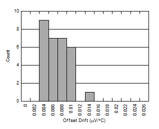
ADS125H02 D037_SBAS790.gif
Gain = 32
Figure 25. Offset Voltage Drift Distribution
ADS125H02 D052_SBAS790.gif
32 units, gain = 0.1875, after calibration
Figure 27. Offset Voltage Long-Term Drift
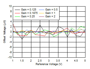
ADS125H02 D013_SBAS790.gif
Gain = 0.125 to 2, after calibration
Figure 29. Offset Voltage vs Reference Voltage
ADS125H02 D040_SBAS790.gif
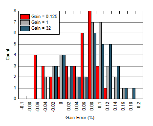
Figure 31. Gain Error Distribution
ADS125H02 D028_SBAS790.gif
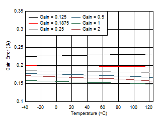
Gain = 0.125 to 2
Figure 33. Gain Error vs Temperature
ADS125H02 D050_SBAS790.gif
32 units, gain = 0.1875, after calibration
Figure 35. Gain Long-Term Drift
ADS125H02 D011_SBAS790.gif
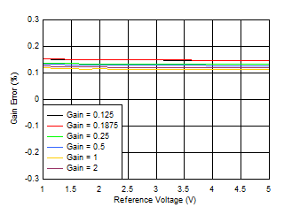
Measurement input range limited to: ±4 V / Gain when VREF > 4 V
Figure 37. Gain Error vs Reference Voltage
ADS125H02 D034_SBAS790.gif
TA = –40°C to +125°C
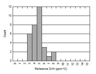
Figure 39. Internal Reference Voltage Drift Distribution
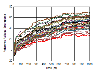
ADS125H02 D048_SBAS790.gif
32 units, normalized data
Figure 41. Internal Reference Voltage Long-Term Drift
ADS125H02 D030_SBAS790.gif
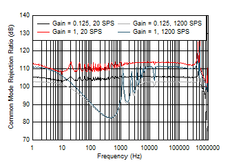
Figure 43. Common-Mode Rejection Ratio vs Frequency
ADS125H02 D019_SBAS760.gif
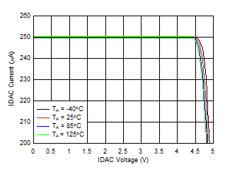
IDAC = 250 µA
Figure 45. IDAC Current vs IDAC Voltage
ADS125H02 D033_SBAS790.gif
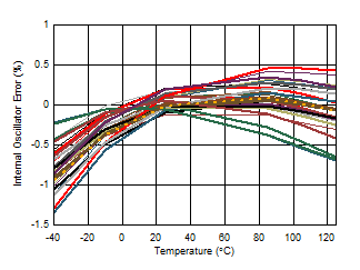
Figure 47. Oscillator Frequency Error vs Temperature
ADS125H02 D031_SBAS790.gif
HV_AVDD and HV_AVSS
Figure 49. PSRR vs Frequency
ADS125H02 D008_SBAS790.gif
All gains
Figure 51. Operating Current vs Temperature