ZHCSIZ6C October   2018  – June 2019 ADS125H02

PRODUCTION DATA.  

  1. 特性
  2. 应用
  3. 说明
    1.     功能方框图
  4. 修订历史记录
  5. Device Comparison Table
  6. Pin Configuration and Functions
    1.     Pin Functions
  7. Specifications
    1. 7.1 Absolute Maximum Ratings
    2. 7.2 ESD Ratings
    3. 7.3 Recommended Operating Conditions
    4. 7.4 Thermal Information
    5. 7.5 Electrical Characteristics
    6. 7.6 Timing Requirements
    7. 7.7 Switching Characteristics
    8. 7.8 Typical Characteristics
  8. Parameter Measurement Information
    1. 8.1 Noise Performance
  9. Detailed Description
    1. 9.1 Overview
    2. 9.2 Functional Block Diagram
    3. 9.3 Feature Description
      1. 9.3.1 Input Range
      2. 9.3.2 Analog Inputs
        1. 9.3.2.1 ESD Diodes
        2. 9.3.2.2 Input Multiplexer
          1. 9.3.2.2.1 Analog Inputs (AIN0, AIN1, AINCOM)
          2. 9.3.2.2.2 High-Voltage Power Supply Readback
          3. 9.3.2.2.3 Internal VCOM Connection (Default)
          4. 9.3.2.2.4 Temperature Sensor
      3. 9.3.3 Programmable Gain Amplifier (PGA)
        1. 9.3.3.1 PGA Operating Range
        2. 9.3.3.2 PGA Monitor
      4. 9.3.4 Reference Voltage
        1. 9.3.4.1 Internal Reference
        2. 9.3.4.2 External Reference
        3. 9.3.4.3 AVDD Power-Supply Reference
        4. 9.3.4.4 Reference Monitor
      5. 9.3.5 Current Sources (IDAC1 and IDAC2)
      6. 9.3.6 General-Purpose Inputs and Outputs (GPIOs)
      7. 9.3.7 ADC Modulator
      8. 9.3.8 Digital Filter
        1. 9.3.8.1 Sinc Filter Mode
          1. 9.3.8.1.1 Sinc Filter Frequency Response
        2. 9.3.8.2 FIR Filter
        3. 9.3.8.3 50-Hz and 60-Hz Normal Mode Rejection
    4. 9.4 Device Functional Modes
      1. 9.4.1 Conversion Control
        1. 9.4.1.1 Continuous-Conversion Mode
        2. 9.4.1.2 Pulse-Conversion Mode
        3. 9.4.1.3 Conversion Latency
        4. 9.4.1.4 Start-Conversion Delay
      2. 9.4.2 Auto-Zero Mode
      3. 9.4.3 Clock Mode
      4. 9.4.4 Reset
        1. 9.4.4.1 Power-On Reset
        2. 9.4.4.2 Reset by Pin
        3. 9.4.4.3 Reset by Command
      5. 9.4.5 Calibration
        1. 9.4.5.1 Offset and Full-Scale Calibration
          1. 9.4.5.1.1 Offset Calibration Registers
          2. 9.4.5.1.2 Full-Scale Calibration Registers
        2. 9.4.5.2 Offset Calibration (OFSCAL)
        3. 9.4.5.3 Full-Scale Calibration (GANCAL)
        4. 9.4.5.4 Calibration Command Procedure
        5. 9.4.5.5 User Calibration Procedure
    5. 9.5 Programming
      1. 9.5.1 Serial Interface
        1. 9.5.1.1 Chip-Select Pins (CS1 and CS2)
        2. 9.5.1.2 Serial Clock (SCLK)
        3. 9.5.1.3 Data Input (DIN)
        4. 9.5.1.4 Data Output/Data Ready (DOUT/DRDY)
      2. 9.5.2 Data Ready (DRDY)
        1. 9.5.2.1 DRDY in Continuous-Conversion Mode
        2. 9.5.2.2 DRDY in Pulse-Conversion Mode
        3. 9.5.2.3 Data Ready by Software Polling
      3. 9.5.3 Conversion Data
        1. 9.5.3.1 Status Byte (STATUS0)
        2. 9.5.3.2 Conversion Data Format
      4. 9.5.4 Cyclic Redundancy Check (CRC)
      5. 9.5.5 Commands
        1. 9.5.5.1  General Command Format
        2. 9.5.5.2  NOP Command
        3. 9.5.5.3  RESET Command
        4. 9.5.5.4  START Command
        5. 9.5.5.5  STOP Command
        6. 9.5.5.6  RDATA Command
        7. 9.5.5.7  OFSCAL Command
        8. 9.5.5.8  GANCAL Command
        9. 9.5.5.9  RREG Command
        10. 9.5.5.10 WREG Command
        11. 9.5.5.11 LOCK Command
        12. 9.5.5.12 UNLOCK Command
    6. 9.6 Register Map
      1. 9.6.1  Device Identification (ID) Register (address = 00h) [reset = 6xh]
        1. Table 30. ID Register Field Descriptions
      2. 9.6.2  Main Status (STATUS0) Register (address = 01h) [reset = 01h]
        1. Table 31. STATUS0 Register Field Descriptions
      3. 9.6.3  Mode 0 (MODE0) Register (address = 02h) [reset = 24h]
        1. Table 32. MODE0 Register Field Descriptions
      4. 9.6.4  Mode 1 (MODE1) Register (address = 03h) [reset = 01h]
        1. Table 33. MODE1 Register Field Descriptions
      5. 9.6.5  Mode 2 (MODE2) Register (address = 04h) [reset = 00h]
        1. Table 34. MODE2 Register Field Descriptions
      6. 9.6.6  Mode 3 (MODE3) Register (address = 05h) [reset = 00h]
        1. Table 35. MODE3 Register Field Descriptions
      7. 9.6.7  Reference Configuration (REF) Register (address = 06h) [reset = 05h]
        1. Table 36. REF Register Field Descriptions
      8. 9.6.8  Offset Calibration (OFCALx) Registers (address = 07h, 08h, 09h) [reset = 00h, 00h, 00h]
        1. Table 37. OFCAL0, OFCAL1, OFCAL2 Registers Field Description
      9. 9.6.9  Full-Scale Calibration (FSCALx) Registers (address = 0Ah, 0Bh, 0Ch) [reset = 00h, 00h, 40h]
        1. Table 38. FSCAL0, FSCAL1, FSCAL2 Registers Field Description
      10. 9.6.10 Current Source Multiplexer (I_MUX) Register (address = 0Dh) [reset = FFh]
        1. Table 39. I_MUX Register Field Descriptions
      11. 9.6.11 Current Source Magnitude (I_MAG) Register (address = 0Eh) [reset = 00h]
        1. Table 40. I_MAG Register Field Descriptions
      12. 9.6.12 Reserved (RESERVED) Register (address = 0Fh) [reset = 00h]
        1. Table 41. RESERVED Register Field Descriptions
      13. 9.6.13 MODE4 (MODE4) Register (address = 10h) [reset = 50h]
        1. Table 42. MODE4 Register Field Descriptions
      14. 9.6.14 PGA Alarm (STATUS1) Register (address = 11h) [reset = xxh]
        1. Table 43. STATUS1 Register Field Descriptions
      15. 9.6.15 Status 2 (STATUS2) Register (address = 12h) [reset = 0xh]
        1. Table 44. STATUS2 Register Field Descriptions
  10. 10Application and Implementation
    1. 10.1 Application Information
      1. 10.1.1 Input Range
      2. 10.1.2 Input Overload
        1. 10.1.2.1 Input Signal Rate of Change (dV/dt)
      3. 10.1.3 Unused Inputs and Outputs
    2. 10.2 Typical Applications
      1. 10.2.1 ±10-V Analog Input Module
        1. 10.2.1.1 Design Requirements
        2. 10.2.1.2 Detailed Design Procedure
        3. 10.2.1.3 Application Curves
      2. 10.2.2 Thermocouple Input With High Common-Mode Voltage
    3. 10.3 Initialization Setup
  11. 11Power Supply Recommendations
    1. 11.1 Power-Supply Decoupling
    2. 11.2 Analog Power-Supply Clamp
    3. 11.3 Power-Supply Sequencing
    4. 11.4 5-V to ±15-V DC-DC Converter
  12. 12Layout
    1. 12.1 Layout Guidelines
    2. 12.2 Layout Example
  13. 13器件和文档支持
    1. 13.1 文档支持
      1. 13.1.1 相关文档
    2. 13.2 接收文档更新通知
    3. 13.3 社区资源
    4. 13.4 商标
    5. 13.5 静电放电警告
    6. 13.6 Glossary
  14. 14机械、封装和可订购信息

Programmable Gain Amplifier (PGA)

The PGA is a low-noise, programmable gain and attenuation, CMOS differential-input, differential-output amplifier. The PGA operates in gain or attenuation mode depending on the gain selected. Typically, the PGA is programmed to provide gain when the expected range of the input signal is less than the reference voltage and is programmed to provide attenuation when the expected range of the input signal is greater than the reference voltage.

Figure 57 shows the block diagram of the PGA.
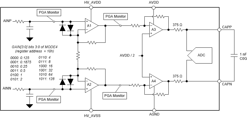
ADS125H02 ads125h02-pga-block-diagram.gifFigure 57. PGA Block Diagram

The PGA inputs are filtered by an RC network to decrease sensitivity to radio frequency interference (RFI) and electromagnetic interference (EMI) interference. The PGA is comprised of two stages: a gain stage followed by an attenuation stage. The first stage is a high input impedance, noninverting differential amplifier (amplifiers A1 and A2) and provides the PGA gain.

The second stage is an inverting, differential amplifier (amplifiers A3 and A4) and provides the attenuation stage. The second stage provides the PGA attenuation for high-amplitude signals. The common-mode voltage of the differential signal is shifted to AVDD / 2. The second stage drives the modulator input of the ADC and is also connected to the CAPP and CAPN pins. An external 1-nF capacitor filters the modulator input sampling pulses and also provides the antialias filter. Place the capacitor close to the pins using short, direct traces. Avoid running clock traces or other digital traces underneath or in the vicinity of these pins.

Amplifiers A1 and A2 have inverse-parallel-connected protection diodes across the amplifiers inputs to clamp the voltage under signal overrange conditions. When the input is overranged, the diodes may conduct resulting in current flow through the diodes, and subsequently, through the analog input pins. Conditions of high dV/dt input signals, such as those generated by the switching of a signal multiplexer, can lead to transient turn-on of the clamp diodes. Use an RC filter at the PGA inputs to limit the dV/dt of the signal to reduce turn-on of the clamp diodes.

The PGA is monitored for high and low operating voltage headroom at four signal points. The output of the eight total monitor outputs are ORed together into a single error bit contained in the conversion data status byte and the STATUS0 register.