ZHCSIZ6C October   2018  – June 2019 ADS125H02

PRODUCTION DATA.  

  1. 特性
  2. 应用
  3. 说明
    1.     功能方框图
  4. 修订历史记录
  5. Device Comparison Table
  6. Pin Configuration and Functions
    1.     Pin Functions
  7. Specifications
    1. 7.1 Absolute Maximum Ratings
    2. 7.2 ESD Ratings
    3. 7.3 Recommended Operating Conditions
    4. 7.4 Thermal Information
    5. 7.5 Electrical Characteristics
    6. 7.6 Timing Requirements
    7. 7.7 Switching Characteristics
    8. 7.8 Typical Characteristics
  8. Parameter Measurement Information
    1. 8.1 Noise Performance
  9. Detailed Description
    1. 9.1 Overview
    2. 9.2 Functional Block Diagram
    3. 9.3 Feature Description
      1. 9.3.1 Input Range
      2. 9.3.2 Analog Inputs
        1. 9.3.2.1 ESD Diodes
        2. 9.3.2.2 Input Multiplexer
          1. 9.3.2.2.1 Analog Inputs (AIN0, AIN1, AINCOM)
          2. 9.3.2.2.2 High-Voltage Power Supply Readback
          3. 9.3.2.2.3 Internal VCOM Connection (Default)
          4. 9.3.2.2.4 Temperature Sensor
      3. 9.3.3 Programmable Gain Amplifier (PGA)
        1. 9.3.3.1 PGA Operating Range
        2. 9.3.3.2 PGA Monitor
      4. 9.3.4 Reference Voltage
        1. 9.3.4.1 Internal Reference
        2. 9.3.4.2 External Reference
        3. 9.3.4.3 AVDD Power-Supply Reference
        4. 9.3.4.4 Reference Monitor
      5. 9.3.5 Current Sources (IDAC1 and IDAC2)
      6. 9.3.6 General-Purpose Inputs and Outputs (GPIOs)
      7. 9.3.7 ADC Modulator
      8. 9.3.8 Digital Filter
        1. 9.3.8.1 Sinc Filter Mode
          1. 9.3.8.1.1 Sinc Filter Frequency Response
        2. 9.3.8.2 FIR Filter
        3. 9.3.8.3 50-Hz and 60-Hz Normal Mode Rejection
    4. 9.4 Device Functional Modes
      1. 9.4.1 Conversion Control
        1. 9.4.1.1 Continuous-Conversion Mode
        2. 9.4.1.2 Pulse-Conversion Mode
        3. 9.4.1.3 Conversion Latency
        4. 9.4.1.4 Start-Conversion Delay
      2. 9.4.2 Auto-Zero Mode
      3. 9.4.3 Clock Mode
      4. 9.4.4 Reset
        1. 9.4.4.1 Power-On Reset
        2. 9.4.4.2 Reset by Pin
        3. 9.4.4.3 Reset by Command
      5. 9.4.5 Calibration
        1. 9.4.5.1 Offset and Full-Scale Calibration
          1. 9.4.5.1.1 Offset Calibration Registers
          2. 9.4.5.1.2 Full-Scale Calibration Registers
        2. 9.4.5.2 Offset Calibration (OFSCAL)
        3. 9.4.5.3 Full-Scale Calibration (GANCAL)
        4. 9.4.5.4 Calibration Command Procedure
        5. 9.4.5.5 User Calibration Procedure
    5. 9.5 Programming
      1. 9.5.1 Serial Interface
        1. 9.5.1.1 Chip-Select Pins (CS1 and CS2)
        2. 9.5.1.2 Serial Clock (SCLK)
        3. 9.5.1.3 Data Input (DIN)
        4. 9.5.1.4 Data Output/Data Ready (DOUT/DRDY)
      2. 9.5.2 Data Ready (DRDY)
        1. 9.5.2.1 DRDY in Continuous-Conversion Mode
        2. 9.5.2.2 DRDY in Pulse-Conversion Mode
        3. 9.5.2.3 Data Ready by Software Polling
      3. 9.5.3 Conversion Data
        1. 9.5.3.1 Status Byte (STATUS0)
        2. 9.5.3.2 Conversion Data Format
      4. 9.5.4 Cyclic Redundancy Check (CRC)
      5. 9.5.5 Commands
        1. 9.5.5.1  General Command Format
        2. 9.5.5.2  NOP Command
        3. 9.5.5.3  RESET Command
        4. 9.5.5.4  START Command
        5. 9.5.5.5  STOP Command
        6. 9.5.5.6  RDATA Command
        7. 9.5.5.7  OFSCAL Command
        8. 9.5.5.8  GANCAL Command
        9. 9.5.5.9  RREG Command
        10. 9.5.5.10 WREG Command
        11. 9.5.5.11 LOCK Command
        12. 9.5.5.12 UNLOCK Command
    6. 9.6 Register Map
      1. 9.6.1  Device Identification (ID) Register (address = 00h) [reset = 6xh]
        1. Table 30. ID Register Field Descriptions
      2. 9.6.2  Main Status (STATUS0) Register (address = 01h) [reset = 01h]
        1. Table 31. STATUS0 Register Field Descriptions
      3. 9.6.3  Mode 0 (MODE0) Register (address = 02h) [reset = 24h]
        1. Table 32. MODE0 Register Field Descriptions
      4. 9.6.4  Mode 1 (MODE1) Register (address = 03h) [reset = 01h]
        1. Table 33. MODE1 Register Field Descriptions
      5. 9.6.5  Mode 2 (MODE2) Register (address = 04h) [reset = 00h]
        1. Table 34. MODE2 Register Field Descriptions
      6. 9.6.6  Mode 3 (MODE3) Register (address = 05h) [reset = 00h]
        1. Table 35. MODE3 Register Field Descriptions
      7. 9.6.7  Reference Configuration (REF) Register (address = 06h) [reset = 05h]
        1. Table 36. REF Register Field Descriptions
      8. 9.6.8  Offset Calibration (OFCALx) Registers (address = 07h, 08h, 09h) [reset = 00h, 00h, 00h]
        1. Table 37. OFCAL0, OFCAL1, OFCAL2 Registers Field Description
      9. 9.6.9  Full-Scale Calibration (FSCALx) Registers (address = 0Ah, 0Bh, 0Ch) [reset = 00h, 00h, 40h]
        1. Table 38. FSCAL0, FSCAL1, FSCAL2 Registers Field Description
      10. 9.6.10 Current Source Multiplexer (I_MUX) Register (address = 0Dh) [reset = FFh]
        1. Table 39. I_MUX Register Field Descriptions
      11. 9.6.11 Current Source Magnitude (I_MAG) Register (address = 0Eh) [reset = 00h]
        1. Table 40. I_MAG Register Field Descriptions
      12. 9.6.12 Reserved (RESERVED) Register (address = 0Fh) [reset = 00h]
        1. Table 41. RESERVED Register Field Descriptions
      13. 9.6.13 MODE4 (MODE4) Register (address = 10h) [reset = 50h]
        1. Table 42. MODE4 Register Field Descriptions
      14. 9.6.14 PGA Alarm (STATUS1) Register (address = 11h) [reset = xxh]
        1. Table 43. STATUS1 Register Field Descriptions
      15. 9.6.15 Status 2 (STATUS2) Register (address = 12h) [reset = 0xh]
        1. Table 44. STATUS2 Register Field Descriptions
  10. 10Application and Implementation
    1. 10.1 Application Information
      1. 10.1.1 Input Range
      2. 10.1.2 Input Overload
        1. 10.1.2.1 Input Signal Rate of Change (dV/dt)
      3. 10.1.3 Unused Inputs and Outputs
    2. 10.2 Typical Applications
      1. 10.2.1 ±10-V Analog Input Module
        1. 10.2.1.1 Design Requirements
        2. 10.2.1.2 Detailed Design Procedure
        3. 10.2.1.3 Application Curves
      2. 10.2.2 Thermocouple Input With High Common-Mode Voltage
    3. 10.3 Initialization Setup
  11. 11Power Supply Recommendations
    1. 11.1 Power-Supply Decoupling
    2. 11.2 Analog Power-Supply Clamp
    3. 11.3 Power-Supply Sequencing
    4. 11.4 5-V to ±15-V DC-DC Converter
  12. 12Layout
    1. 12.1 Layout Guidelines
    2. 12.2 Layout Example
  13. 13器件和文档支持
    1. 13.1 文档支持
      1. 13.1.1 相关文档
    2. 13.2 接收文档更新通知
    3. 13.3 社区资源
    4. 13.4 商标
    5. 13.5 静电放电警告
    6. 13.6 Glossary
  14. 14机械、封装和可订购信息

PGA Operating Range

As with many amplifiers, the PGA limits the absolute input voltage that must not be exceeded in the linear operating range. The absolute voltage is the combined differential and common-mode voltages. The maximum allowable absolute voltage is determined by the PGA gain, the maximum differential input voltage (VIN), and the minimum value of the high-voltage power supply. Maintain the absolute input voltage (VAINX) within the range as shown in Equation 5, otherwise incorrect conversion data can result:

Equation 5. HV_AVSS + 2.5 + VIN × (Gain – 1) / 2 < V(AINx) < HV_AVDD – 2.5 – VIN × (Gain – 1) / 2

where

  • For gain < 1, use value = 1 for gain
  • V(AINx) = Absolute input voltage
  • VIN = VAINP – VAINN = Maximum expected differential input voltage

The differential input signal can also be limited by two other conditions. The first limiting condition is when the reference voltage exceeds AVDD – 1 V (nominally VREF > 4 V). In this case, the differential input signal is limited to: VIN = ±(AVDD – 1 V) / Gain, instead of the ideal VIN = ±VREF / Gain. The second limiting condition applies to gains of 0.125 and 0.1875. In this case, the differential input signal is limited to: VIN = ±20 V, regardless of the reference voltage.

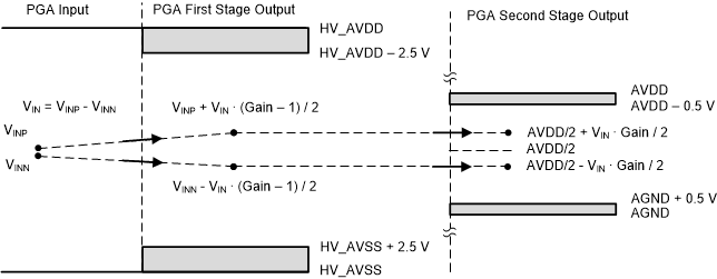
Figure 58 and Figure 59 show the relationship between the PGA input voltage to the PGA output voltage. In attenuation mode, the first PGA stage is configured as a unity-gain follower. The second PGA stage attenuates the differential input and shifts the signal common-mode voltage to AVDD / 2 to drive the ADC input.

In gain mode, the first PGA stage amplifies the differential signal. The second PGA stage is configured as a unity-gain follower with level-shift. Figure 58 and Figure 59 show the corresponding output voltage of the PGA stages that must have operating voltage headroom.
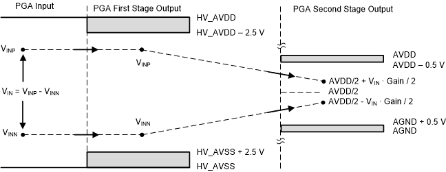
ADS125H02 ads125h02-pga-attenuation.gifFigure 58. PGA Attenuation Mode
ADS125H02 ads125h02-pga-gain.gifFigure 59. PGA Gain Mode