ZHCSJ23C November   2018  – September 2019 UCC20225-Q1 , UCC20225A-Q1

PRODUCTION DATA.  

  1. 特性
  2. 应用
  3. 说明
    1.     Device Images
      1.      功能方框图
  4. 修订历史记录
  5. Pin Configuration and Functions
    1.     Pin Functions
  6. Specifications
    1. 6.1  Absolute Maximum Ratings
    2. 6.2  ESD Ratings
    3. 6.3  Recommended Operating Conditions
    4. 6.4  Thermal Information
    5. 6.5  Power Ratings
    6. 6.6  Insulation Specifications
    7. 6.7  Safety-Related Certifications
    8. 6.8  Safety Limiting Values
    9. 6.9  Electrical Characteristics
    10. 6.10 Switching Characteristics
    11. 6.11 Thermal Derating Curves
    12. 6.12 Typical Characteristics
  7. Parameter Measurement Information
    1. 7.1 Propagation Delay and Pulse Width Distortion
    2. 7.2 Rising and Falling Time
    3. 7.3 PWM Input and Disable Response Time
    4. 7.4 Programable Dead Time
    5. 7.5 Power-up UVLO Delay to OUTPUT
    6. 7.6 CMTI Testing
  8. Detailed Description
    1. 8.1 Overview
    2. 8.2 Functional Block Diagram
    3. 8.3 Feature Description
      1. 8.3.1 VDD, VCCI, and Under Voltage Lock Out (UVLO)
      2. 8.3.2 Input and Output Logic Table
      3. 8.3.3 Input Stage
      4. 8.3.4 Output Stage
      5. 8.3.5 Diode Structure in UCC20225-Q1 family
    4. 8.4 Device Functional Modes
      1. 8.4.1 Disable Pin
      2. 8.4.2 Programmable Dead Time (DT) Pin
        1. 8.4.2.1 Tying the DT Pin to VCC
        2. 8.4.2.2 DT Pin Left Open or Connected to a Programming Resistor between DT and GND Pins
  9. Application and Implementation
    1. 9.1 Application Information
    2. 9.2 Typical Application
      1. 9.2.1 Design Requirements
      2. 9.2.2 Detailed Design Procedure
        1. 9.2.2.1 Designing PWM Input Filter
        2. 9.2.2.2 Select External Bootstrap Diode and its Series Resistor
        3. 9.2.2.3 Gate Driver Output Resistor
        4. 9.2.2.4 Estimate Gate Driver Power Loss
        5. 9.2.2.5 Estimating Junction Temperature
        6. 9.2.2.6 Selecting VCCI, VDDA/B Capacitor
          1. 9.2.2.6.1 Selecting a VCCI Capacitor
          2. 9.2.2.6.2 Selecting a VDDA (Bootstrap) Capacitor
          3. 9.2.2.6.3 Select a VDDB Capacitor
        7. 9.2.2.7 Dead Time Setting Guidelines
        8. 9.2.2.8 Application Circuits with Output Stage Negative Bias
      3. 9.2.3 Application Curves
  10. 10Power Supply Recommendations
  11. 11Layout
    1. 11.1 Layout Guidelines
    2. 11.2 Layout Example
  12. 12器件和文档支持
    1. 12.1 相关链接
    2. 12.2 文档支持
      1. 12.2.1 相关文档
    3. 12.3 认证
    4. 12.4 接收文档更新通知
    5. 12.5 社区资源
    6. 12.6 商标
    7. 12.7 静电放电警告
    8. 12.8 Glossary
  13. 13机械、封装和可订购信息

PWM Input and Disable Response Time

Figure 28 shows the response time of the disable function. For more information, see Disable Pin.
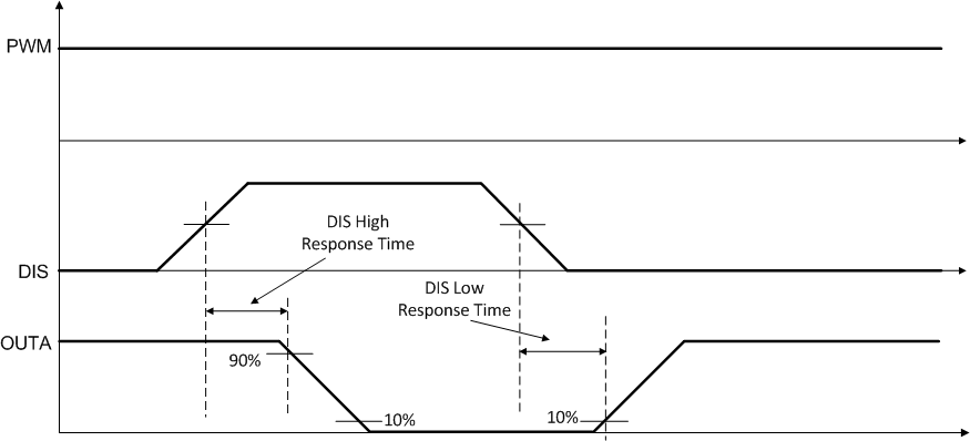
UCC20225-Q1 UCC20225A-Q1 fig28_sluscn0.gifFigure 28. Disable Pin Timing