ZHCSJ38C December 2018 – August 2019 TPS3840
PRODUCTION DATA.
- 1 特性
- 2 应用
- 3 说明
- 4 修订历史记录
- 5 Device Comparison Table
- 6 Pin Configuration and Functions
- 7 Specifications
- 8 Detailed Description
-
9 Application and Implementation
- 9.1 Application Information
- 9.2 Typical Application
- 10Power Supply Recommendations
- 11Layout
- 12器件和文档支持
- 13机械、封装和可订购信息
7.6 Timing Requirements
At 1.5 V ≤ VDD ≤ 10 V, CT = MR = Open, RESET pull-up resistor (Rpull-up) = 100 kΩ to VDD, output reset load (CLOAD) = 10 pF and over the operating free-air temperature range – 40°C to 125°C, VDD slew rate < 100mV / us, unless otherwise noted. Typical values are at TJ = 25°C.| PARAMETER | TEST CONDITIONS | MIN | TYP | MAX | UNIT | |
|---|---|---|---|---|---|---|
| tSTRT | Startup Delay(1) | CT pin open | 100 | 220 | 350 | µs |
| tP_HL | Propagation detect delay for VDD falling below VIT- | VDD = VIT+ to (VIT-) - 10%(2) | 15 | 30 | µs | |
| tD | Reset time delay | CT pin = open
|
50 | µs | ||
| CT pin = 10 nF | 6.2 | ms | ||||
| CT pin = 1 µF | 619 | ms | ||||
| tGI_VIT- | Glitch immunity VIT- | 5% VIT- overdrive(3) | 10 | µs | ||
| tMR_PW | MR pin pulse duration to initiate reset | 300 | ns | |||
| tMR_RES | Propagation delay from MR low to reset | VDD = 4.5 V, MR < VMR_L | 700 | ns | ||
| tMR_tD | Delay from release MR to deasert reset | VDD = 4.5 V,
MR = VMR_L to VMR_H |
tD | ms | ||

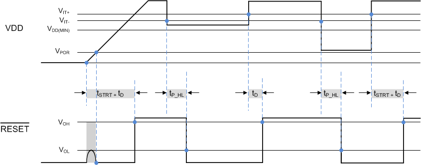
1. tD (no cap) is included in tSTRT time delay. If tD delay is programmed by an external capacitor connected to CT pin then tD programmed time will be added to the startup time, VDD slew rate = 100 mV / µs.
2. Open-Drain timing diagram assumes pull-up resistor is connected to RESET
3. RESET output is undefined when VDD is < VPOR
Figure 3. Timing Diagram TPS3840DL (Open-Drain Active-Low) 
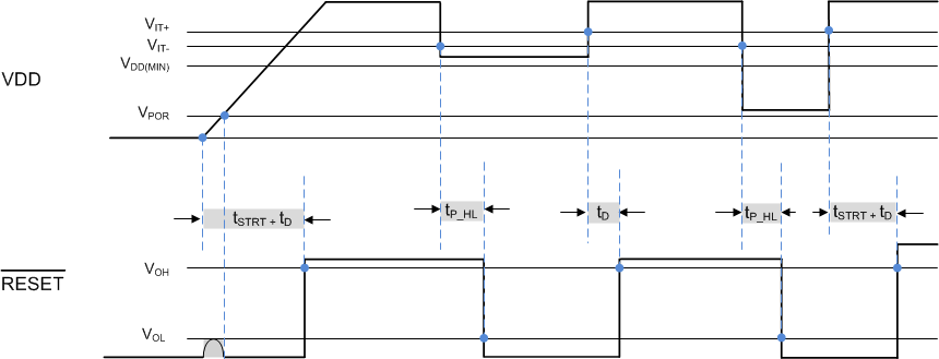
1. tD (no cap) is included in tSTRT time delay. If tD delay is programmed by an external capacitor connected to CT pin, then tD programmed time will be added to the startup time. VDD slew rate = 100 mV / µs.
2. RESET output is undefined when VDD < VPOR and limited to VOL for VDD slew rate = 100 mV / µs
Figure 4. Timing Diagram TPS3840PL (Push-Pull Active-Low) 
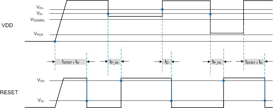
1. tD (no cap) is included in tSTRT time delay. If tD delay is programmed by an external capacitor connected to CT pin, then tD programmed time will be added to the total startup time. VDD slew rate = 100 mV / µs.
Figure 5. Timing Diagram TPS3840PH (Push-Pull Active-High)