ZHCSJ40 December 2018 DAC8742H
PRODUCTION DATA.
- 1 特性
- 2 应用
- 3 说明
- 4 修订历史记录
- 5 Pin Configuration and Functions
- 6 Specifications
-
7 Detailed Description
- 7.1 Overview
- 7.2 Functional Block Diagram
- 7.3
Feature Description
- 7.3.1 HART Modulator
- 7.3.2 HART Demodulator
- 7.3.3 FOUNDATION FIELDBUS / PROFIBUS PA Manchester Encoder
- 7.3.4 FOUNDATION FIELDBUS / PROFIBUS PA Manchester Decoder
- 7.3.5 Internal Reference
- 7.3.6 Clock Configuration
- 7.3.7 Reset and Power-Down
- 7.3.8 Full-Duplex Mode
- 7.3.9 I/O Selection
- 7.3.10 Jabber Inhibitor
- 7.4 Device Functional Modes
- 7.5
Register Maps
- 7.5.1 CONTROL Register (Offset = 2h) [reset = 0x8042]
- 7.5.2 RESET Register (Offset = 7h) [reset = 0x0000]
- 7.5.3 MODEM_STATUS Register (Offset = 20h) [reset = 0x0000]
- 7.5.4 MODEM_IRQ_MASK Register (Offset = 21h) [reset = 0x0024]
- 7.5.5 MODEM_CONTROL Register (Offset = 22h) [reset = 0x0048]
- 7.5.6 FIFO_D2M Register (Offset = 23h) [reset = 0x0200]
- 7.5.7 FIFO_M2D Register (Offset = 24h) [reset = 0x0200]
- 7.5.8 FIFO_LEVEL_SET Register (Offset = 25h) [reset = 0x0000]
- 7.5.9 PAFF_JABBER Register (Offset = 27h) [reset = 0x0000]
- 8 Application and Implementation
- 9 Power Supply Recommendations
- 10Layout
- 11器件和文档支持
- 12机械、封装和可订购信息
8.1.3 Included Functions and Filter Selection
As a highly integrated device, the DAC8742H not only includes the modulation and demodulation capabilities for the previously described industrial protocols, but also includes an internal reference, and integrated receive bandpass filter, with other aforementioned functions. In HART mode, an internal amplifier provides high output drive capability, and can drive a wide range of purely capacitive loads, ranging from 5 nF to 22 nF. The lower value specified in the load range is to ensure output stability. Two different filter configurations, external and internal, are achievable through the BPF_EN digital input -- logic high on this pin enables the internal bandpass filter. The external filter configuration is shown in Figure 32. The example provided displays the DAC8742H device configured with an external reference and external bandpass filter.
 Figure 32. HART Mode: DAC8742H Passive Selection For External Bandpass Filter and External Reference
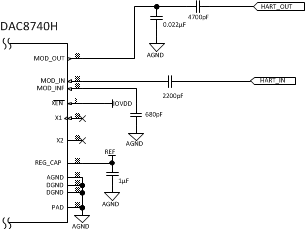
 The second configuration, which can reduce costs associated with PCB development and BOM component counts, additionally aids in the optimization of board space. This optimization gives the user flexibility into achieving industrial applications with smaller form factor sizes. The internal filter configuration, with correct MOD_IN, MOD_INF, and MOD_OUT connections, is shown in Figure 33.
 Figure 33. HART Mode: DAC8742H Passive Selection For Internal Filter