ZHCSJ89B January 2019 – July 2022 ADS8353-Q1
PRODUCTION DATA
- 1特性
- 2应用
- 3说明
- 4Revision History
- 5Pin Configuration and Functions
- 6Specifications
- 7Detailed Description
- 8Application and Implementation
- 9Device and Documentation Support
8.1.2 Charge Kickback Filter
Converting analog-to-digital signals requires sampling an input signal at a constant rate. Any higher frequency content in the input signal beyond half the sampling frequency is digitized and folded back into the low-frequency spectrum. This process is called aliasing. Therefore, an analog, charge kickback filter must be used to remove the harmonic content from the input signal before being sampled by the ADC. A charge kickback filter is designed as a low-pass, RC filter, for which the 3-dB bandwidth is optimized based on specific application requirements. For dc signals with fast transients (including multiplexed input signals), a high-bandwidth filter is designed to allow accurately settling the signal at the ADC inputs during the small acquisition time window. For ac signals, keep the filter bandwidth low to band-limit the noise fed into the ADC input, thereby increasing the signal-to-noise ratio (SNR) of the system.
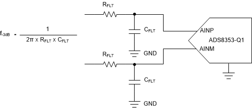
A filter capacitor, CFLT, connected across the ADC inputs (see Figure 8-1), filters the noise from the front-end drive circuitry, reduces the sampling charge injection, and provides a charge bucket to quickly charge the internal sample-and-hold capacitors during the acquisition process. As a rule of thumb, the value of this capacitor must be at least 10 times the specified value of the ADC sampling capacitance. For these devices, the input sampling capacitance is equal to 40 pF. Thus, the value of CFLT must be greater than 400 pF. The capacitor must be a COG- or NPO-type because these capacitor types have a high-Q, low-temperature coefficient, and stable electrical characteristics under varying voltages, frequency, and time.
 Figure 8-1 Charge Kickback Filter
Driving capacitive loads can degrade the phase margin of the input amplifiers, thus making the amplifier marginally unstable. To avoid amplifier stability issues, series isolation resistors (RFLT) are used at the output of the amplifiers. A higher value of RFLT is helpful from the amplifier stability perspective, but adds distortion as a result of interactions with the nonlinear input impedance of the ADC. Distortion increases with source impedance, input signal frequency, and input signal amplitude. Therefore, the selection of RFLT requires balancing the stability and distortion of the design. For more information on ADC input R-C filter component selection, see the TI Precision Labs on ti.com.