ZHCSJ89B January 2019 – July 2022 ADS8353-Q1
PRODUCTION DATA
- 1特性
- 2应用
- 3说明
- 4Revision History
- 5Pin Configuration and Functions
- 6Specifications
- 7Detailed Description
- 8Application and Implementation
- 9Device and Documentation Support
7.3.3 Transfer Function
The device supports two input configurations:
- Single-ended inputs, CFR.B7 = 0 (default), or
- Pseudo-differential inputs, CFR.B7 = 1
The device also supports two output data formats:
- Straight binary output, CFR.B4 = 0 (default), or
- Two's compliment output, CFR.B4 = 1
Equation 5 calculates the device resolution:
Equation 5. 1 LSB = (FSR_ADC_x) / (2N)
where:
- N = 16
- FSR_ADC_x = the full-scale input range of the ADC (see the Section 7.3.2 section for more details)
Table 7-2 and Table 7-3 show the different input voltages and the corresponding output codes from the device.
Table 7-2 Transfer Characteristics for Straight Binary Output (CFR.B4 = 0, Default)
| INPUT CONFIGURATION | INPUT VOLTAGE | OUTPUT CODE (Hex) | |||
|---|---|---|---|---|---|
| STRAIGHT BINARY (CFR.B4 = 0, Default) | |||||
| AINP_x | AINM_x | AINP_x - AINM_x | CODE | ADS8353-Q1 | |
| Single-ended (CFR.B7 = 0, default) | ≤ 1 LSB | 0 | ≤ 1 LSB | ZC | 0000 |
| FSR_ADC_x / 2 | FSR_ADC_x / 2 | MC | 7FFF | ||
| ≥ FSR_ADC_x – 1 LSB | ≥ FSR_ADC_x – 1 LSB | FSC | FFFF | ||
| Pseudo-differential (CFR.B7 = 1) | ≤ 1 LSB | FSR_ADC_x / 2 | ≤ –FSR_ADC_x / 2 + 1 LSB | ZC | 0000 |
| FSR_ADC_x / 2 | 0 | MC | 7FFF | ||
| ≥ FSR_ADC_x – 1 LSB | ≥ FSR_ADC_x / 2 – 1 LSB | FSC | FFFF | ||
Table 7-3 Transfer Characteristics for Two's Compliment Output (CFR.B4 = 1)
| INPUT CONFIGURATION | INPUT VOLTAGE | OUTPUT CODE (Hex) | |||
|---|---|---|---|---|---|
| TWO'S COMPLIMENT (CFR.B4 = 1, Default) | |||||
| AINP_x | AINM_x | AINP_x - AINM_x | CODE | ADS8353-Q1 | |
| Single-ended (CFR.B7 = 0, default) | ≤ 1 LSB | 0 | ≤ 1 LSB | NFSC | 8000 |
| FSR_ADC_x / 2 | FSR_ADC_x / 2 | MC | 0000 | ||
| ≥ FSR_ADC_x – 1 LSB | ≥ FSR_ADC_x – 1 LSB | PFSC | 7FFF | ||
| Pseudo-differential (CFR.B7 = 1) | ≤ 1 LSB | FSR_ADC_x / 2 | ≤ –FSR_ADC_x / 2 + 1 LSB | NFSC | 8000 |
| FSR_ADC_x / 2 | 0 | MC | 0000 | ||
| ≥ FSR_ADC_x – 1 LSB | ≥ FSR_ADC_x / 2 – 1 LSB | PFSC | 7FFF | ||
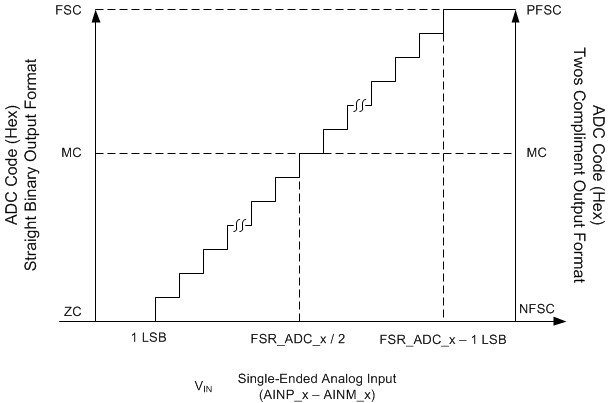
Figure 7-3 shows the ideal device transfer characteristics for the single-ended analog input.
 Figure 7-3 Ideal Transfer Characteristics for a Single-Ended Analog Input
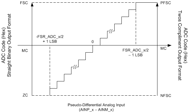
Figure 7-4 shows the ideal device transfer characteristics for the pseudo-differential analog input.
 Figure 7-4 Ideal Transfer Characteristics for a Pseudo-Differential Analog Input