ZHCSJB4D April 2019 – January 2024 TAS2563
PRODUCTION DATA
- 1
- 1 特性
- 2 应用
- 3 说明
- 4 Pin Configuration and Functions
-
5 Specifications
- 5.1 Absolute Maximum Ratings
- 5.2 ESD Ratings
- 5.3 Recommended Operating Conditions
- 5.4 Thermal Information
- 5.5 Electrical Characteristics
- 5.6 I2C Timing Requirements
- 5.7 SPI Timing Requirements
- 5.8 PDM Port Timing Requirements
- 5.9 TDM Port Timing Requirements
- 5.10 Timing Diagrams
- 5.11 Typical Characteristics
- 6 Parameter Measurement Information
-
7 Detailed Description
- 7.1 Overview
- 7.2 Functional Block Diagram
- 7.3
Feature Description
- 7.3.1 PurePath Console 3 Software
- 7.3.2 Device Mode and Address Selection
- 7.3.3 General I2C Operation
- 7.3.4 General SPI Operation
- 7.3.5 Single-Byte and Multiple-Byte Transfers
- 7.3.6 Single-Byte Write
- 7.3.7 Multiple-Byte Write and Incremental Multiple-Byte Write
- 7.3.8 Single-Byte Read
- 7.3.9 Multiple-Byte Read
- 7.3.10 Register Organization
- 7.3.11 Operational Modes
- 7.3.12 Faults and Status
- 7.3.13 Digital Input Pull Downs
- 7.4 Device Functional Modes
- 7.5
Register Maps
- 7.5.1 Register Summary Table Page=0x00
- 7.5.2 PAGE (page=0x00 address=0x00) [reset=0h]
- 7.5.3 SW_RESET (page=0x00 address=0x01) [reset=0h]
- 7.5.4 PWR_CTL (page=0x00 address=0x02) [reset=Eh]
- 7.5.5 PB_CFG1 (page=0x00 address=0x03) [reset=20h]
- 7.5.6 MISC_CFG1 (page=0x00 address=0x04) [reset=C6h]
- 7.5.7 MISC_CFG2 (page=0x00 address=0x05) [reset=22h]
- 7.5.8 TDM_CFG0 (page=0x00 address=0x06) [reset=9h]
- 7.5.9 TDM_CFG1 (page=0x00 address=0x07) [reset=2h]
- 7.5.10 TDM_CFG2 (page=0x00 address=0x08) [reset=4Ah]
- 7.5.11 TDM_CFG3 (page=0x00 address=0x09) [reset=10h]
- 7.5.12 TDM_CFG4 (page=0x00 address=0x0A) [reset=13h]
- 7.5.13 TDM_CFG5 (page=0x00 address=0x0B) [reset=2h]
- 7.5.14 TDM_CFG6 (page=0x00 address=0x0C) [reset=0h]
- 7.5.15 TDM_CFG7 (page=0x00 address=0x0D) [reset=4h]
- 7.5.16 TDM_CFG8 (page=0x00 address=0x0E) [reset=5h]
- 7.5.17 TDM_CFG9 (page=0x00 address=0x0F) [reset=6h]
- 7.5.18 TDM_CFG10 (page=0x00 address=0x10) [reset=7h]
- 7.5.19 DSP Mode & TDM_DET (page=0x00 address=0x11) [reset=7Fh]
- 7.5.20 LIM_CFG0 (page=0x00 address=0x12) [reset=12h]
- 7.5.21 LIM_CFG1 (page=0x00 address=0x13) [reset=76h]
- 7.5.22 DSP FREQUENCY & BOP_CFG0 (page=0x00 address=0x14) [reset=1h]
- 7.5.23 BOP_CFG0 (page=0x00 address=0x15) [reset=2Eh]
- 7.5.24 BIL_and_ICLA_CFG0 (page=0x00 address=0x16) [reset=60h]
- 7.5.25 BIL_ICLA_CFG1 (page=0x00 address=0x17) [reset=0h]
- 7.5.26 GAIN_ICLA_CFG0 (page=0x00 address=0x18) [reset=0h]
- 7.5.27 ICLA_CFG1 (page=0x00 address=0x19) [reset=0h]
- 7.5.28 INT_MASK0 (page=0x00 address=0x1A) [reset=FCh]
- 7.5.29 INT_MASK1 (page=0x00 address=0x1B) [reset=A6h]
- 7.5.30 INT_MASK2 (page=0x00 address=0x1C) [reset=DFh]
- 7.5.31 INT_MASK3 (page=0x00 address=0x1D) [reset=FFh]
- 7.5.32 INT_LIVE0 (page=0x00 address=0x1F) [reset=0h]
- 7.5.33 INT_LIVE1 (page=0x00 address=0x20) [reset=0h]
- 7.5.34 INT_LIVE3 (page=0x00 address=0x21) [reset=0h]
- 7.5.35 INT_LIVE4 (page=0x00 address=0x22) [reset=0h]
- 7.5.36 INT_LTCH0 (page=0x00 address=0x24) [reset=0h]
- 7.5.37 INT_LTCH1 (page=0x00 address=0x25) [reset=0h]
- 7.5.38 INT_LTCH3 (page=0x00 address=0x26) [reset=0h]
- 7.5.39 INT_LTCH4 (page=0x00 address=0x27) [reset=0h]
- 7.5.40 VBAT_MSB (page=0x00 address=0x2A) [reset=0h]
- 7.5.41 VBAT_LSB (page=0x00 address=0x2B) [reset=0h]
- 7.5.42 TEMP (page=0x00 address=0x2C) [reset=0h]
- 7.5.43 INT & CLK CFG (page=0x00 address=0x30) [reset=19h]
- 7.5.44 DIN_PD (page=0x00 address=0x31) [reset=40h]
- 7.5.45 MISC (page=0x00 address=0x32) [reset=80h]
- 7.5.46 BOOST_CFG1 (page=0x00 address=0x33) [reset=34h]
- 7.5.47 BOOST_CFG2 (page=0x00 address=0x34) [reset=4Bh]
- 7.5.48 BOOST_CFG3 (page=0x00 address=0x35) [reset=74h]
- 7.5.49 MISC (page=0x00 address=0x3B) [reset=58h]
- 7.5.50 TG_CFG0 (page=0x00 address=0x3F) [reset=0h]
- 7.5.51 BST_ILIM_CFG0 (page=0x00 address=0x40) [reset=36h]
- 7.5.52 PDM_CONFIG0 (page=0x00 address=0x41) [reset=1h]
- 7.5.53 DIN_PD & PDM_CONFIG3 (page=0x00 address=0x42) [reset=F8h]
- 7.5.54 ASI2_CONFIG0 (page=0x00 address=0x43) [reset=8h]
- 7.5.55 ASI2_CONFIG1 (page=0x00 address=0x44) [reset=0h]
- 7.5.56 ASI2_CONFIG2 (page=0x00 address=0x45) [reset=1h]
- 7.5.57 ASI2_CONFIG3 (page=0x00 address=0x46) [reset=FCh]
- 7.5.58 PVDD_MSB_DSP (page=0x00 address=0x49) [reset=0h]
- 7.5.59 PVDD_LSB_DSP (page=0x00 address=0x4A) [reset=0h]
- 7.5.60 REV_ID (page=0x00 address=0x7D) [reset=0h]
- 7.5.61 I2C_CKSUM (page=0x00 address=0x7E) [reset=0h]
- 7.5.62 BOOK (page=0x00 address=0x7F) [reset=0h]
- 8 Application and Implementation
- 9 Power Supply Recommendations
- 10Layout
- 11Device and Documentation Support
- 12Revision History
- 13Mechanical, Packaging, and Orderable Information
7.4.6 IV Sense
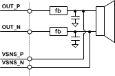
The TAS2563 provides speaker voltage and current sense for real time monitoring of loudspeaker behavior. The VSNS_P and VSNS_N pins should be connected after any ferrite bead filter (or directly to the OUT_P and OUT_N connections if no EMI filter is used). The V-Sense connections eliminate IR drop error due to packaging, PCB interconnect or ferrite bead filter resistance. It should be noted that any interconnect resistance after the V-Sense terminals will not be corrected for, so it is advised to connect the sense connections as close to the load as possible.
 Figure 7-20 V-Sense Connections
I-Sense and V-Sense can be powered down by asserting the ISNS_PD and VSNS_PD register bits respectively. When powered down, the device will return null samples for the powered down block. The IV-sense is High Pass Filtered and the Bi-Quad filter coefficients can be changed from the default 2 Hz using the IVHPFC_N0, IVHPFC_N1, IVHPFC_D1 registers using the equations [N, D] = butter(1, fc/(fs/2), 'high'); round(N(0)*2^31);. These coefficients can be calculated and set using Section 7.3.1.
| ISNS_PD | SETTING |
|---|---|
| I-Sense is active |
| I-Sense is powered down (default) |
| VSNS_PD | SETTING |
|---|---|
| V-Sense is active |
| V-Sense is powered down (default) |