ZHCSJB4D April 2019 – January 2024 TAS2563
PRODUCTION DATA
- 1
- 1 特性
- 2 应用
- 3 说明
- 4 Pin Configuration and Functions
-
5 Specifications
- 5.1 Absolute Maximum Ratings
- 5.2 ESD Ratings
- 5.3 Recommended Operating Conditions
- 5.4 Thermal Information
- 5.5 Electrical Characteristics
- 5.6 I2C Timing Requirements
- 5.7 SPI Timing Requirements
- 5.8 PDM Port Timing Requirements
- 5.9 TDM Port Timing Requirements
- 5.10 Timing Diagrams
- 5.11 Typical Characteristics
- 6 Parameter Measurement Information
-
7 Detailed Description
- 7.1 Overview
- 7.2 Functional Block Diagram
- 7.3
Feature Description
- 7.3.1 PurePath Console 3 Software
- 7.3.2 Device Mode and Address Selection
- 7.3.3 General I2C Operation
- 7.3.4 General SPI Operation
- 7.3.5 Single-Byte and Multiple-Byte Transfers
- 7.3.6 Single-Byte Write
- 7.3.7 Multiple-Byte Write and Incremental Multiple-Byte Write
- 7.3.8 Single-Byte Read
- 7.3.9 Multiple-Byte Read
- 7.3.10 Register Organization
- 7.3.11 Operational Modes
- 7.3.12 Faults and Status
- 7.3.13 Digital Input Pull Downs
- 7.4 Device Functional Modes
- 7.5
Register Maps
- 7.5.1 Register Summary Table Page=0x00
- 7.5.2 PAGE (page=0x00 address=0x00) [reset=0h]
- 7.5.3 SW_RESET (page=0x00 address=0x01) [reset=0h]
- 7.5.4 PWR_CTL (page=0x00 address=0x02) [reset=Eh]
- 7.5.5 PB_CFG1 (page=0x00 address=0x03) [reset=20h]
- 7.5.6 MISC_CFG1 (page=0x00 address=0x04) [reset=C6h]
- 7.5.7 MISC_CFG2 (page=0x00 address=0x05) [reset=22h]
- 7.5.8 TDM_CFG0 (page=0x00 address=0x06) [reset=9h]
- 7.5.9 TDM_CFG1 (page=0x00 address=0x07) [reset=2h]
- 7.5.10 TDM_CFG2 (page=0x00 address=0x08) [reset=4Ah]
- 7.5.11 TDM_CFG3 (page=0x00 address=0x09) [reset=10h]
- 7.5.12 TDM_CFG4 (page=0x00 address=0x0A) [reset=13h]
- 7.5.13 TDM_CFG5 (page=0x00 address=0x0B) [reset=2h]
- 7.5.14 TDM_CFG6 (page=0x00 address=0x0C) [reset=0h]
- 7.5.15 TDM_CFG7 (page=0x00 address=0x0D) [reset=4h]
- 7.5.16 TDM_CFG8 (page=0x00 address=0x0E) [reset=5h]
- 7.5.17 TDM_CFG9 (page=0x00 address=0x0F) [reset=6h]
- 7.5.18 TDM_CFG10 (page=0x00 address=0x10) [reset=7h]
- 7.5.19 DSP Mode & TDM_DET (page=0x00 address=0x11) [reset=7Fh]
- 7.5.20 LIM_CFG0 (page=0x00 address=0x12) [reset=12h]
- 7.5.21 LIM_CFG1 (page=0x00 address=0x13) [reset=76h]
- 7.5.22 DSP FREQUENCY & BOP_CFG0 (page=0x00 address=0x14) [reset=1h]
- 7.5.23 BOP_CFG0 (page=0x00 address=0x15) [reset=2Eh]
- 7.5.24 BIL_and_ICLA_CFG0 (page=0x00 address=0x16) [reset=60h]
- 7.5.25 BIL_ICLA_CFG1 (page=0x00 address=0x17) [reset=0h]
- 7.5.26 GAIN_ICLA_CFG0 (page=0x00 address=0x18) [reset=0h]
- 7.5.27 ICLA_CFG1 (page=0x00 address=0x19) [reset=0h]
- 7.5.28 INT_MASK0 (page=0x00 address=0x1A) [reset=FCh]
- 7.5.29 INT_MASK1 (page=0x00 address=0x1B) [reset=A6h]
- 7.5.30 INT_MASK2 (page=0x00 address=0x1C) [reset=DFh]
- 7.5.31 INT_MASK3 (page=0x00 address=0x1D) [reset=FFh]
- 7.5.32 INT_LIVE0 (page=0x00 address=0x1F) [reset=0h]
- 7.5.33 INT_LIVE1 (page=0x00 address=0x20) [reset=0h]
- 7.5.34 INT_LIVE3 (page=0x00 address=0x21) [reset=0h]
- 7.5.35 INT_LIVE4 (page=0x00 address=0x22) [reset=0h]
- 7.5.36 INT_LTCH0 (page=0x00 address=0x24) [reset=0h]
- 7.5.37 INT_LTCH1 (page=0x00 address=0x25) [reset=0h]
- 7.5.38 INT_LTCH3 (page=0x00 address=0x26) [reset=0h]
- 7.5.39 INT_LTCH4 (page=0x00 address=0x27) [reset=0h]
- 7.5.40 VBAT_MSB (page=0x00 address=0x2A) [reset=0h]
- 7.5.41 VBAT_LSB (page=0x00 address=0x2B) [reset=0h]
- 7.5.42 TEMP (page=0x00 address=0x2C) [reset=0h]
- 7.5.43 INT & CLK CFG (page=0x00 address=0x30) [reset=19h]
- 7.5.44 DIN_PD (page=0x00 address=0x31) [reset=40h]
- 7.5.45 MISC (page=0x00 address=0x32) [reset=80h]
- 7.5.46 BOOST_CFG1 (page=0x00 address=0x33) [reset=34h]
- 7.5.47 BOOST_CFG2 (page=0x00 address=0x34) [reset=4Bh]
- 7.5.48 BOOST_CFG3 (page=0x00 address=0x35) [reset=74h]
- 7.5.49 MISC (page=0x00 address=0x3B) [reset=58h]
- 7.5.50 TG_CFG0 (page=0x00 address=0x3F) [reset=0h]
- 7.5.51 BST_ILIM_CFG0 (page=0x00 address=0x40) [reset=36h]
- 7.5.52 PDM_CONFIG0 (page=0x00 address=0x41) [reset=1h]
- 7.5.53 DIN_PD & PDM_CONFIG3 (page=0x00 address=0x42) [reset=F8h]
- 7.5.54 ASI2_CONFIG0 (page=0x00 address=0x43) [reset=8h]
- 7.5.55 ASI2_CONFIG1 (page=0x00 address=0x44) [reset=0h]
- 7.5.56 ASI2_CONFIG2 (page=0x00 address=0x45) [reset=1h]
- 7.5.57 ASI2_CONFIG3 (page=0x00 address=0x46) [reset=FCh]
- 7.5.58 PVDD_MSB_DSP (page=0x00 address=0x49) [reset=0h]
- 7.5.59 PVDD_LSB_DSP (page=0x00 address=0x4A) [reset=0h]
- 7.5.60 REV_ID (page=0x00 address=0x7D) [reset=0h]
- 7.5.61 I2C_CKSUM (page=0x00 address=0x7E) [reset=0h]
- 7.5.62 BOOK (page=0x00 address=0x7F) [reset=0h]
- 8 Application and Implementation
- 9 Power Supply Recommendations
- 10Layout
- 11Device and Documentation Support
- 12Revision History
- 13Mechanical, Packaging, and Orderable Information
7.4.3.6 Supply Tracking Limiters with Brown Out Prevention
The TAS2563 monitors battery voltage (VBAT) and the class-D voltage (PVDD) along with the audio signal to automatically decrease gain when the audio signal peaks exceed a programmable threshold. This helps prevent clipping and extends playback time through end of charge battery conditions. The limiters threshold can be configured to track the monitored voltage below a programmable inflection point with a programmable slope. A minimum threshold sets the limit of threshold reduction from the voltage tracking. Configurable attack rate, hold time and release rate are provided to shape the dynamic response of each limiter. The total attenuation is the sum of both the VBAT and PVDD limiter. If the ICLA is enabled the actual attenuation is based on the ICLA configuration using the calculated attenuation value of all devices on the selected ICLA bus.
A Brown Out Prevention (BOP) feature provides a priority input to provide a very fast response to transient dips in the battery supply (VBAT) which at end of charge conditions that can cause system level brown out. When the selected supply dips below the brown-out threshold the BOP will begin reducing gain with an first attack latency of less than 10 µs and a configurable attack rate. When the VBAT supply rises above the brownout threshold, the BOP will begin to release after the programmed hold time. During a BOP event the limiter updates will be paused. This is to prevent a limiter from releasing during a BOP event. The VBAT and PVDD limiters are enabled by setting the respective LIMB_EN and LIMP_EN bits high.
| LIMB_EN | VALUE |
|---|---|
| Disabled (default) |
| Enabled |
| LIMP_EN | VALUE |
|---|---|
| Disabled (default) |
| Enabled |
The limiters have configurable attack rates, hold times and release rates, which are available via the LIMB_ATK_RT[2:0], LIMB_HLD_TM[2:0], LIMB_RLS_RT[2:0] register bits respectively for VBAT and LIMP_ATK_RT[2:0], LIMP_HLD_TM[2:0], LIMP_RLS_RT[2:0] register bits respectively for PVDD . The limiters attack and release step sizes can be set by configuring the LIMB_ATK_ST[1:0] and LIMB_RLS_ST[1:0] register bits respectively for VBAT and LIMP_ATK_ST[1:0] and LIMP_RLS_ST[1:0] register bits respectively for PVDD. For sampling rates less that 44.1kHz and greater than 8 kHz the minimum attack rate is 20µs and for sampling rates of 8kHz or less the minimum attack rate is 40µs.
A maximum level of attenuation applied by the limiters and brown out prevention feature is configurable via the LIM_MAX_ATN register. This attenuation limit is shared between the features. For instance, if the maximum attenuation is set to 6 dB and the limiters have reduced gain by 4 dB, the brown out prevention feature will only be able to reduce the gain further by another 2 dB. If the limiter or brown out prevention feature is attacking and it reaches the maximum attenuation, gain will not be reduced any further.
The limiter max attenuation LIM_MAX_ATN represent the limit in a 1.X format. To calculate the value to write to the 4 registers by apply the following formula to the desired dB using equation LIMB_MAX_ATN = round(10^(-dB/20)*2^31).
| LIM_MAX_ATN[31:0] | ATTENUATION (dB) |
|---|---|
| -1 |
| ... |
| -9 (default) |
| ... |
| -16.5 |
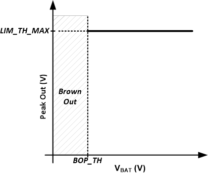
The limiter begins reducing gain when the output signal level is greater than the limiter threshold. The limiter can be configured to track selected supply below a programmable inflection point with a minimum threshold value. Figure 7-15 below shows the limiter configured to limit to a constant level regardless of the selected supply level. To achieve this behavior, set the limiter maximum threshold to the desired level using LIM_TH_MAX. Set the limiter inflection point using LIM_INF_PT below the minimum allowable supply setting. The limiter minimum threshold register LIM_TH_MIN does not impact limiter behavior in this use case.
 Figure 7-15 Limiter with Fixed Threshold
The VBAT limiter threshold max LIMB_TH_MAX and min LIMB_TH_MIN registers represent the limit in a 5.X format. To calculate the value to write to the 4 registers by apply the following formula to the desired threshold voltage using the equation LIMB_TH_MAX or LIMB_TH_MIN = round(Volts*2^27).
| LIMB_TH_MAX[31:0] | THRESHOLD (V) |
|---|---|
| 2.5 |
| ... |
| 9 (default) |
| ... |
| 15.5 |
| LIMB_TH_MIN[31:0] | THRESHOLD (V) |
|---|---|
| 2.5 |
| ... |
| 4 (default) |
| ... |
| 15.5 |
The VBAT limiter inflection point LIMB_INF_PT represent the limit in a 5.X format. To calculate the value to write to the 4 registers by apply the following formula to the desired infection voltage using the equation LIMB_INF_PT = round(Volts*2^27).
| LIMB_INF_PT[31:0] | THRESHOLD (V) |
|---|---|
| 2 |
| ... |
| 3.3 (default) |
| ... |
| 6 |
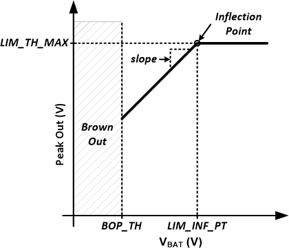
Figure 7-16 shows how to configure the limiter to track selected supply below a threshold without a minimum threshold. Set the LIM_TH_MAX register to the desired threshold and LIM_INF_PT register to the desired inflection point where the limiter will begin reducing the threshold with the selected supply. The default value of 1 V/V will reduce the threshold 1 V for every 1 V of drop in the supply voltage. More aggressive tracking slopes can be programmed if desired. Program the LIM_TH_MIN below the minimum the selected supply to prevent the limiter from having a minimum threshold reduction when tracking the selected supply.
The VBAT limiter tracking slope LIMB_SLOPE[31:0] represent the limit in a 5.X format. To calculate the value to write to the 4 registers by apply the following formula to the desired infection voltage using equation LIMB_SLOPE = round(slope(V/V)*2^27)
 Figure 7-16 Limiter with Inflection Point
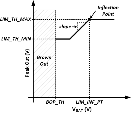
To achieve a limiter that tracks the selected supply below a threshold, configure the limiter as explained in the previous example, except program the LIM_TH_MIN register to the desired minimum threshold. This is shown in Figure 7-17 below.
 Figure 7-17 Limiter with Inflection Point and Minimum Threshold
The TAS2563 also employs a Brown Out Prevention (BOP) feature that serves as a low latency priority input to the limiter engine that begins attacking the VBAT supply dipping below the programmed BOP threshold. This feature can be enabled by setting the BOP_EN register bit high. It should be noted that the BOP feature is independent of the limiter and will function if enabled, even if the limiter is disabled. The BOP threshold is configured by setting the threshold with register bits BOP_TH.
| BOP_EN | VALUE |
|---|---|
| Disabled |
| Enabled (default) |
The Brownout prevention threshold BOP_TH represent a threshold in a 5.X format. To calculate the value to write to the 4 registers by apply the following formula to the desired brownout threshold using equation BOP_TH = round(Volts*2^27).
| BOP_TH[31:0] | VBAT THRESHOLD (V) |
|---|---|
| Reserved |
| 2.5 |
| ... |
| 2.9 (default) |
| ... |
| 4 |
| Reserved |
The BOP feature has a separate attack rate BOP_ATK_RT, attack step size BOP_ATK_ST and hold time BOP_HLD_TM from the battery tracking limiter. The BOP feature uses the LIMB_RLS_RT register setting to release after a brown out event. The rates are based on the number of audio samples and actual time values can be calculated by multiplying by 1/fs. For example the attack rate of 4 samples at 48 ksps would be approximately 83 µs.
| BOP_ATK_RT[2:0] | ATTACK RATE (samples/step) | ATTACK RATE @ 48 ksps (~µs) |
|---|---|---|
| 1 | 20 |
| 2 | 42 |
| 4 | 83 |
| 8 | 167 |
| 16 | 333 |
| 32 | 666 |
| 64 | 1300 |
| 128 | 2700 |
| BOP_ATK_ST[1:0] | STEP SIZE (dB) |
|---|---|
| 0.5 |
| 1 (default) |
| 1.5 |
| 2 |
| BOP_HLD_TM[2:0] | HOLD TIME (ms) |
|---|---|
| 0 |
| 10 |
| 25 |
| 50 |
| 100 |
| 250 |
| 500 (default) |
| 1000 |
The TAS2563 can also shutdown the device when a brown out event occurs if the BOP_MUTE register bit is set high. For the device to continue playing audio again, the device must transition through a SW/HW shutdown state. Setting the BOP_INF_HLD high will cause the limiter to stay in the hold state (i.e. never release) after a cleared brown out event until either the device transitions through a mute or SW/HW shutdown state or the register bit BOP_HLD_CLR is written to a high value (which will cause the device to exit the hold state and begin releasing). This bit is self clearing and will always readback low. Figure 7-18 below illustrates the entering and exiting from a brown out event.
 Figure 7-18 Brown Out Prevention Event
| BOP_MUTE | VALUE |
|---|---|
| Don't Shutdown (default) |
| Mute then shutdown |
| BOP_INF_HLD | VALUE |
|---|---|
| Use BOP_HLD_TM after Brown Out event (default) |
| Do not release until BOP_HLD_CLR is asserted high |
| BOP_HLD_CLR | VALUE |
|---|---|
| Don't clear (default) |
| Clear event (self clearing) |
A hard brownout level can be set to shutdown the TAS2563 if the BOP cannot mitigate the drop in battery voltage VBAT. This will shutdown the device and should not be used if the BOP_MUTE is enable. The brownout shutdown will only function if brownout engine is enabled using BOP_EN.
| BOSD_EN | VALUE |
|---|---|
| Disabled (default) |
| Enabled |
The Brownout prevention shutdown threshold BOSD_TH represent a threshold in a 5.X format. To calculate the value to write to the 4 registers by apply the following formula to the desired brownout threshold using equation BOSD_TH = round(Volts*2^27).
| BOSD_TH[31:0] | VBAT THRESHOLD (V) |
|---|---|
| 2.5 |
| ... |
| 2.7 (default) |
| ... |
| 3.99 |