ZHCSJF8F December 2008 – April 2019 TPS61175
PRODUCTION DATA.
- 1 特性
- 2 应用
- 3 说明
- 4 修订历史记录
- 5 Pin Configuration and Functions
- 6 Specifications
- 7 Detailed Description
-
8 Application and Implementation
- 8.1 Application Information
- 8.2
Typical Application
- 8.2.1 Design Requirements
- 8.2.2
Detailed Design Procedure
- 8.2.2.1 Custom Design with WEBENCH Tools
- 8.2.2.2 Determining the Duty Cycle
- 8.2.2.3 Selecting the Inductor
- 8.2.2.4 Computing the Maximum Output Current
- 8.2.2.5 Setting Output Voltage
- 8.2.2.6 Setting the Switching Frequency
- 8.2.2.7 Setting the Soft-Start Time
- 8.2.2.8 Selecting the Schottky Diode
- 8.2.2.9 Selecting the Input and Output Capacitors
- 8.2.2.10 Compensating the Small Signal Control Loop
- 8.2.3 Application Curves
- 9 Power Supply Recommendations
- 10Layout
- 11器件和文档支持
- 12机械、封装和可订购信息
8.2.2.5 Setting Output Voltage
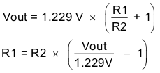
To set the output voltage in either DCM or CCM, select the values of R1 and R2 according to Equation 9:
Equation 9. 

Considering the leakage current through the resistor divider and noise decoupling into FB pin, an optimum value for R2 is around 10 k. The output voltage tolerance depends on the VFB accuracy and the tolerance of R1 and R2.