ZHCSJG2A March 2019 – September 2019 TPS7A78
PRODUCTION DATA.
- 1 特性
- 2 应用
- 3 说明
- 4 修订历史记录
- 5 Pin Configuration and Functions
- 6 Specifications
-
7 Detailed Description
- 7.1 Overview
- 7.2 Functional Block Diagram
- 7.3
Feature Description
- 7.3.1 Active Bridge Control
- 7.3.2 Full-Bridge (FB) and Half-Bridge (HB) Configurations
- 7.3.3 4:1 Switched-Capacitor Voltage Reduction
- 7.3.4 Undervoltage Lockout Circuits (VUVLO_SCIN) and (VUVLO_LDO_IN)
- 7.3.5 Dropout Voltage Regulation
- 7.3.6 Current Limit
- 7.3.7 Programmable Power-Fail Detection
- 7.3.8 Power-Good (PG) Detection
- 7.3.9 Thermal Shutdown
- 7.4 Device Functional Modes
-
8 Application and Implementation
- 8.1
Application Information
- 8.1.1 Recommended Capacitor Types
- 8.1.2 Input and Output Capacitors Requirements
- 8.1.3 Startup Behavior
- 8.1.4 Load Transient
- 8.1.5 Standby Power and Output Efficiency
- 8.1.6 Reverse Current
- 8.1.7 Switched-Capacitor Stage Output Impedance
- 8.1.8 Power Dissipation (PD)
- 8.1.9 Estimating Junction Temperature
- 8.2
Typical Application
- 8.2.1 Design Requirements
- 8.2.2
Detailed Design Procedure
- 8.2.2.1 Calculating the Cap-Drop Capacitor CS
- 8.2.2.2 Calculating the Surge Resistor RS
- 8.2.2.3 Checking for the Device Maximum ISHUNT Current
- 8.2.2.4 Calculating the Bulk Capacitor CSCIN
- 8.2.2.5 Calculating the PFD Pin Resistor Dividers for a Power-Fail Detection
- 8.2.2.6 Summary of the Typical Application Design Components
- 8.2.3 Application Curves
- 8.1
Application Information
- 9 Power Supply Recommendations
- 10Layout
- 11器件和文档支持
- 12机械、封装和可订购信息
8.1.5 Standby Power and Output Efficiency
The AC input current cannot be directly calculated because of the active bridge control; see the Active Bridge Control section. The AC input current through the AC+ and AC– pins is a combination of two current components, as shown in Figure 24: ISHUNT and IPEAK. The ISHUNT current component is identified by its wave profile because this component is the AC charging current supplied by the cap-drop capacitor CS. The IPEAK current component is identified by its instantaneous peak current profile.
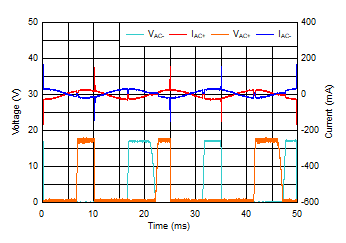 Figure 24. The Device VAC Input Current With its Two Components
 Equation 1 calculates the shunt current ISHUNT, and Equation 2 calculates the peak current IPEAK.
where
- VAC (MAX) is the maximum VAC supply RMS voltage
- XCS is the impedance of the standard CS capacitor to be used in the application
- VSCIN is the rectified DC voltage on the SCIN pin
- RS is the standard RS resistor to be used in the application
The frequency of the shunt activity is uncorrelated to the AC input frequency. Therefore, the standby power must be measured with a power analyzer. Fortunately, using a power analyzer is relatively simple and the measurement setup shown in Figure 25 and Figure 26 can be used to measure the standby power and the output efficiency.
If the application has an upstream current-limit circuit that limits any high-transient input currents, such as surge or hot-plug currents, the requirement for the surge resistor RS can be relaxed. The input transient current-limit circuit allows the RS resistor to be removed, thus significantly improving the standby power and output efficiency because no power loss is dissipated in RS.
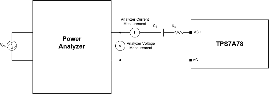 Figure 25. Standby Power and Output Efficiency Measurement Setup
  Figure 26. Standby Power and Output Efficiency Measurement Setup With an Upstream Current-Limit Circuit
 The standby power and output efficiency measurements shown in Figure 27 to Figure 29 were created with the measurement setup in Figure 25.
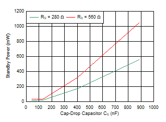
| VAC = 120 VRMS at 60 Hz, FB, VLDO_OUT = 5.0 V,
IOUT = 0 mA |
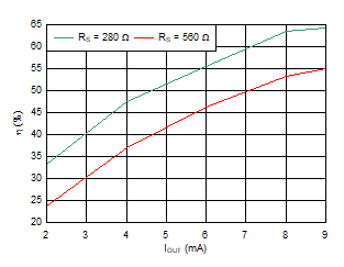
| VAC = 120 VRMS at 60 Hz, HB, CS = 150 nF, VLDO_OUT = 5.0 V |
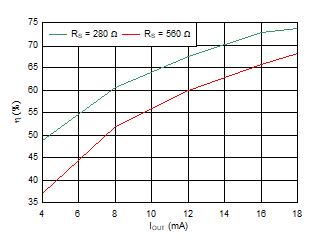
| VAC = 120 VRMS at 60 Hz, FB, CS = 150 nF, VLDO_OUT = 5.0 V |