ZHCSJG2A March 2019 – September 2019 TPS7A78
PRODUCTION DATA.
- 1 特性
- 2 应用
- 3 说明
- 4 修订历史记录
- 5 Pin Configuration and Functions
- 6 Specifications
-
7 Detailed Description
- 7.1 Overview
- 7.2 Functional Block Diagram
- 7.3
Feature Description
- 7.3.1 Active Bridge Control
- 7.3.2 Full-Bridge (FB) and Half-Bridge (HB) Configurations
- 7.3.3 4:1 Switched-Capacitor Voltage Reduction
- 7.3.4 Undervoltage Lockout Circuits (VUVLO_SCIN) and (VUVLO_LDO_IN)
- 7.3.5 Dropout Voltage Regulation
- 7.3.6 Current Limit
- 7.3.7 Programmable Power-Fail Detection
- 7.3.8 Power-Good (PG) Detection
- 7.3.9 Thermal Shutdown
- 7.4 Device Functional Modes
-
8 Application and Implementation
- 8.1
Application Information
- 8.1.1 Recommended Capacitor Types
- 8.1.2 Input and Output Capacitors Requirements
- 8.1.3 Startup Behavior
- 8.1.4 Load Transient
- 8.1.5 Standby Power and Output Efficiency
- 8.1.6 Reverse Current
- 8.1.7 Switched-Capacitor Stage Output Impedance
- 8.1.8 Power Dissipation (PD)
- 8.1.9 Estimating Junction Temperature
- 8.2
Typical Application
- 8.2.1 Design Requirements
- 8.2.2
Detailed Design Procedure
- 8.2.2.1 Calculating the Cap-Drop Capacitor CS
- 8.2.2.2 Calculating the Surge Resistor RS
- 8.2.2.3 Checking for the Device Maximum ISHUNT Current
- 8.2.2.4 Calculating the Bulk Capacitor CSCIN
- 8.2.2.5 Calculating the PFD Pin Resistor Dividers for a Power-Fail Detection
- 8.2.2.6 Summary of the Typical Application Design Components
- 8.2.3 Application Curves
- 8.1
Application Information
- 9 Power Supply Recommendations
- 10Layout
- 11器件和文档支持
- 12机械、封装和可订购信息
8.1.7 Switched-Capacitor Stage Output Impedance
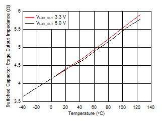
To ensure a low output impedance of the device switched-capacitor stage (charge pump), connect a 1-µF X5R or a better dielectric capacitor in parallel with the bulk capacitor CSCIN. Figure 32 shows the switched-capacitor stage output impedance versus temperature at the maximum output current of 120 mA. When a DC supply power source is used to power the device under heavy loading conditions close to the maximum current rating at high temperature, the load can run the LDO into dropout because of the degradation in the charge pump output impedance. To enhance performance with a DC supply, apply the DC supply voltage to the SCIN pin equal to 4 (VLDO_OUT (nom) + 0.6 V) + 2 V to ensure optimal performance. See Figure 5 and Figure 6 for a 3.3-V output voltage example.
 Figure 32. Switched-Capacitor Stage Output Impedance vs Temperature at a 120-mA Load Current