ZHCSJH3A March 2019 – November 2023 INA185
PRODUCTION DATA
- 1
- 1 特性
- 2 应用
- 3 说明
- 4 Pin Configuration and Functions
- 5 Specifications
- 6 Detailed Description
- 7 Application and Implementation
- 8 Device and Documentation Support
- 9 Revision History
- 10Mechanical, Packaging, and Orderable Information
7.3.1 Common-Mode Transients Greater Than 26 V
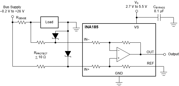
With a small amount of additional circuitry, the INA185 can be used in circuits that are subjected to transients higher than 26 V, such as automotive applications. Use only Zener diodes or Zener-type transient absorbers (sometimes referred to as transorbs)—any other type of transient absorber has an unacceptable time delay. Start by adding a pair of resistors as a working impedance for the Zener diode. See Figure 7-5. Keep these resistors as small as possible; most often, around 10 Ω. Larger values can be used with an effect on gain that is discussed in the Signal Filtering section. This circuit limits only short-term transients, therefore many applications are satisfied with a 10-Ω resistor along with conventional Zener diodes of the lowest acceptable power rating. This combination uses the least amount of board space. These diodes can be found in packages as small as SOT-523 or SOD-523.
 Figure 7-5 Transient Protection Using Dual Zener Diodes
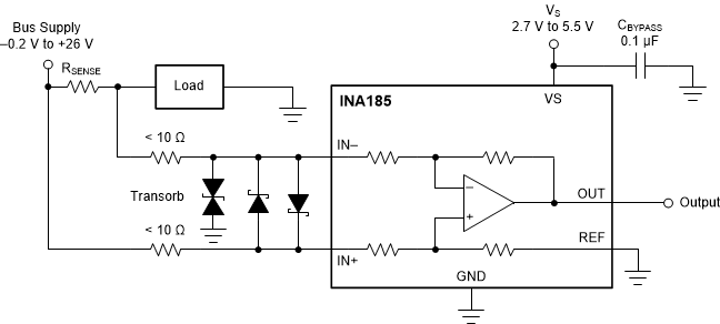
In the event that low-power Zener diodes do not have sufficient transient absorption capability, a higher-power transorb must be used. The most package-efficient solution involves using a single transorb and back-to-back diodes between the device inputs, as shown in Figure 7-6. The most space-efficient solutions are dual, series-connected diodes in a single SOT-523 or SOD-523 package. In either of the examples shown in Figure 7-5 and Figure 7-6, the total board area required by the INA185 with all protective components is less than that of an SO-8 package, and only slightly greater than that of an MSOP-8 package.
 Figure 7-6 Transient Protection
Using a Single Transorb and Input Clamps
Figure 7-6 Transient Protection
Using a Single Transorb and Input ClampsFor more information, see the Current Shunt Monitor With Transient Robustness reference design.