ZHCSJL9B April   2019  – April 2019 TPS566235

PRODUCTION DATA.  

  1. 特性
  2. 应用
  3. 说明
    1.     Device Images
      1.      典型应用
      2.      效率与输出电流 Eco-mode
  4. 修订历史记录
  5. Pin Configuration and Functions
    1.     Pin Functions
  6. Specifications
    1. 6.1 Absolute Maximum Ratings
    2. 6.2 ESD Ratings
    3. 6.3 Recommended Operating Conditions
    4. 6.4 Thermal Information
    5. 6.5 Electrical Characteristics
    6. 6.6 Typical Characteristics
  7. Detailed Description
    1. 7.1 Overview
    2. 7.2 Functional Block Diagram
    3. 7.3 Feature Description
      1. 7.3.1 PWM Operation and D-CAP3 Control
      2. 7.3.2 Power Good
      3. 7.3.3 Soft Start and Pre-Biased Soft Start
      4. 7.3.4 Over current Protection and Undervoltage Protection
      5. 7.3.5 Over Voltage Protection
      6. 7.3.6 UVLO Protection
      7. 7.3.7 Thermal Shutdown
    4. 7.4 Device Functional Modes
      1. 7.4.1 Light Load Operation
      2. 7.4.2 MODE Pin Configuration
      3. 7.4.3 Advanced Eco-Mode Control
      4. 7.4.4 Out-Of-Audio Mode
      5. 7.4.5 Force CCM Mode
      6. 7.4.6 Standby Operation
  8. Application and Implementation
    1. 8.1 Application Information
    2. 8.2 Typical Application
      1. 8.2.1 Design Requirements
      2. 8.2.2 Detailed Design Procedure
        1. 8.2.2.1 Custom Design With WEBENCH® Tools
        2. 8.2.2.2 Inductor Selection
        3. 8.2.2.3 Output Capacitor Selection
        4. 8.2.2.4 Input Capacitor Selection
      3. 8.2.3 Application Curves
  9. Power Supply Recommendations
  10. 10Layout
    1. 10.1 Layout Guidelines
    2. 10.2 Layout Example
  11. 11器件和文档支持
    1. 11.1 器件支持
      1. 11.1.1 第三方米6体育平台手机版_好二三四免责声明
      2. 11.1.2 开发支持
        1. 11.1.2.1 使用 WEBENCH® 工具创建定制设计
    2. 11.2 接收文档更新通知
    3. 11.3 社区资源
    4. 11.4 商标
    5. 11.5 静电放电警告
    6. 11.6 术语表
  12. 12机械、封装和可订购信息

Typical Characteristics

TJ=-40oC to 125oC, VIN=12V(unless otherwise noted)
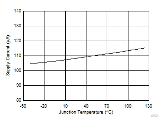
TPS566235 D002-SupplyCurrent.gif
VEN = 5 V
Figure 1. Supply Current vs Junction Temperature
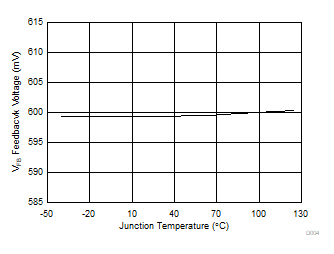
TPS566235 D004-VFBFeedbacvkVoltage.gif
Figure 3. Feedback Voltage vs Junction Temperature
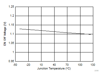
TPS566235 D006-ENOffVoltage.gif
Figure 5. Enable Off Voltage vs Junction Temperature
TPS566235 D008-Low-SideRDS(on).gif
Figure 7. Low-Side RDS(on) vs Junction Temperature
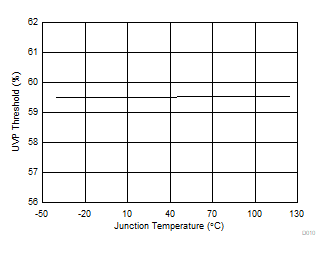
TPS566235 D010-UVPThreshold.gif
Figure 9. UVP Threshold vs Junction Temperature
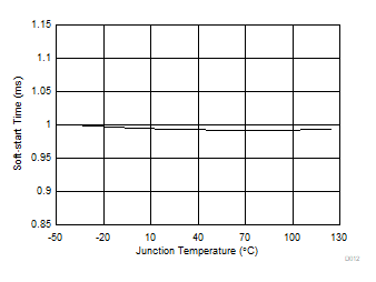
TPS566235 D012-Soft-startTime.gif
Figure 11. Soft-Start Time vs Junction Temperature
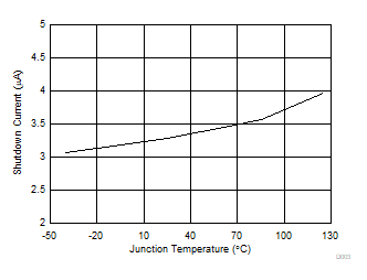
TPS566235 D003-ShutdownCurrent.gif
VEN = 0 V
Figure 2. Shutdown Current vs Temperature
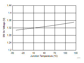
TPS566235 D005-ENOnVoltage.gif
Figure 4. Enable On Voltage vs Junction Temperature
TPS566235 D007-High-SideRDS(on).gif
Figure 6. High-Side RDS(on) vs Junction Temperature
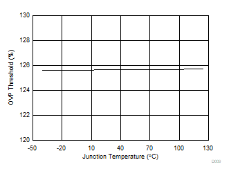
TPS566235 D009-OVPThreshold.gif
Figure 8. OVP Threshold vs Junction Temperature
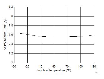
TPS566235 D011-ValleyCurrentLimit.gif
Figure 10. Valley Current Limit vs Junction Temperature
TPS566235 D013-EfficiencyPSM.gif
Figure 12. Efficiency, Eco-mode
TPS566235 D014-EfficiencyFCCM.gif
Figure 14. Efficiency, FCCM
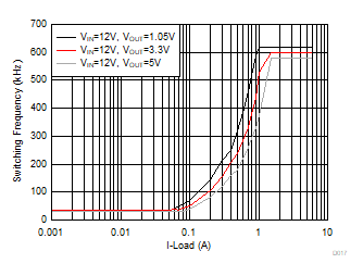
TPS566235 D017-FswOOA.gif
Figure 16. Switching Frequency vs Output Load, OOA-mode
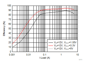
TPS566235 D015-EfficiencyOOA.gif
Figure 13. Efficiency, OOA-mode
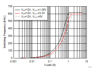
TPS566235 D023-EfficiencyPSM.gif
Figure 15. Switching Frequency vs Output Load, Eco-mode
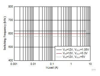
TPS566235 D018-FswFCCM.gif
Figure 17. Switching Frequency vs Output Load, FCCM