ZHCSJO2C May   2019  – April 2020 TPS7B81-Q1

PRODUCTION DATA.  

  1. 特性
  2. 应用
  3. 说明
    1.     Device Images
      1.      典型应用原理图
  4. 修订历史记录
  5. Pin Configuration and Functions
    1.     Pin Functions
  6. Specifications
    1. 6.1 Absolute Maximum Ratings
    2. 6.2 ESD Ratings
    3. 6.3 Recommended Operating Conditions
    4. 6.4 Thermal Information
    5. 6.5 Electrical Characteristics
    6. 6.6 Typical Characteristics
  7. Detailed Description
    1. 7.1 Overview
    2. 7.2 Functional Block Diagram
    3. 7.3 Feature Description
      1. 7.3.1 Device Enable (EN)
      2. 7.3.2 Undervoltage Shutdown
      3. 7.3.3 Current Limit
      4. 7.3.4 Thermal Shutdown
    4. 7.4 Device Functional Modes
      1. 7.4.1 Operation With VIN Lower Than 3 V
      2. 7.4.2 Operation With VIN Larger Than 3 V
  8. Application and Implementation
    1. 8.1 Application Information
      1. 8.1.1 Power Dissipation
        1. 8.1.1.1 Estimating Junction Temperature
    2. 8.2 Typical Application
      1. 8.2.1 Design Requirements
      2. 8.2.2 Detailed Design Procedure
        1. 8.2.2.1 Input Capacitor
        2. 8.2.2.2 Output Capacitor
      3. 8.2.3 Application Curve
  9. Power Supply Recommendations
  10. 10Layout
    1. 10.1 Layout Guidelines
    2. 10.2 Layout Example
  11. 11器件和文档支持
    1. 11.1 接收文档更新通知
    2. 11.2 支持资源
    3. 11.3 商标
    4. 11.4 静电放电警告
    5. 11.5 Glossary
  12. 12机械、封装和可订购信息

Typical Application

Figure 31 shows a typical application circuit for the TPS7B81-Q1. Different external component values can be used, depending on the end application. An application may require a larger output capacitor during fast load steps to prevent a large drop on the output voltage. TI recommends using a low-equivalent series resistance (ESR) ceramic capacitor with an X5R- or X7R-type dielectric.
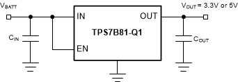
TPS7B81-Q1 tps7b81_q1.gifFigure 31. TPS7B81-Q1 Typical Application Schematic