ZHCSJZ2D August 2019 – April 2021 THS6222
PRODUCTION DATA
8.2.1.2 Detailed Design Procedure
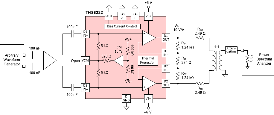
The closed-loop gain equation for a differential line driver such as the THS6222 is given as AV = 1 + 2 × (RF / RG), where RF = RF1 = RF2. The THS6222 is a current-feedback amplifier and thus the bandwidth of the closed-loop configuration is set by the value of the RF resistor. This advantage of the current-feedback architecture allows for flexibility in setting the differential gain by choosing the value of the RG resistor without reducing the bandwidth as is the case with voltage-feedback amplifiers. The THS6222 is designed to provide optimal bandwidth performance with RF1 = RF2 = 1.24 kΩ. To configure the device in a gain of 10 V/V, the RG resistor is chosen to be 274 Ω. See the TI Precision Labs for more details on how to choose the RF resistor to optimize the performance of a current-feedback amplifier.
Often, a key requirement for PLC applications is the out-of-band suppression specifications. The in-band frequencies carry the encoded data with a certain power level. The line driver must not generate any spurs beyond a certain power level outside the in-band spectrum. In the design requirements of this application example, the minimum out-of-band suppression specification of 35 dB means there must be no frequency spurs in the out-of-band spectrum beyond the –80 dBm/Hz power spectral density, considering the in-band power spectral density is –50 dBm/Hz.
The circuit shown in Figure 8-2 measures the out-of-band suppression specification. The minor difference in components between the circuits of Figure 8-1 and Figure 8-2 does not have any significant impact on the out-of-band suppression results.
 Figure 8-2 Measurement Test Circuit for
Out-of-Band Suppression