ZHCSJZ2D August   2019  – April 2021 THS6222

PRODUCTION DATA  

  1. 特性
  2. 应用
  3. 说明
  4. Revision History
  5. Pin Configuration and Functions
  6. Specifications
    1. 6.1 Absolute Maximum Ratings
    2. 6.2 ESD Ratings
    3. 6.3 Recommended Operating Conditions
    4. 6.4 Thermal Information
    5. 6.5 Electrical Characteristics: VS = 12 V
    6. 6.6 Electrical Characteristics: VS = 32 V
    7. 6.7 Timing Requirements
    8. 6.8 Typical Characteristics: VS = 12 V
    9. 6.9 Typical Characteristics: VS = 32 V
  7. Detailed Description
    1. 7.1 Overview
    2. 7.2 Functional Block Diagram
    3. 7.3 Feature Description
      1. 7.3.1 Common-Mode Buffer
      2. 7.3.2 Thermal Protection and Package Power Dissipation
      3. 7.3.3 Output Voltage and Current Drive
      4. 7.3.4 Breakdown Supply Voltage
      5. 7.3.5 Surge Test Results
    4. 7.4 Device Functional Modes
  8. Application and Implementation
    1. 8.1 Application Information
    2. 8.2 Typical Applications
      1. 8.2.1 Broadband PLC Line Driving
        1. 8.2.1.1 Design Requirements
        2. 8.2.1.2 Detailed Design Procedure
        3. 8.2.1.3 Application Curve
    3. 8.3 What to Do and What Not to Do
      1. 8.3.1 Do
      2. 8.3.2 Do Not
  9. Power Supply Recommendations
  10. 10Layout
    1. 10.1 Layout Guidelines
    2. 10.2 Wafer and Die Information
    3. 10.3 Layout Examples
  11. 11Device and Documentation Support
    1. 11.1 Development Support
    2. 11.2 Documentation Support
      1. 11.2.1 Related Documentation
    3. 11.3 Receiving Notification of Documentation Updates
    4. 11.4 支持资源
    5. 11.5 Trademarks
    6. 11.6 Electrostatic Discharge Caution
    7. 11.7 Glossary
  12. 12Mechanical, Packaging, and Orderable Information

Typical Characteristics: VS = 32 V

At TA ≈ 25°C, AV = 10 V/V, RF = 1.24 kΩ, RL = 100 Ω, RS = 2.5 Ω, RADJ = 0 Ω, full-bias mode, and VCM = open (unless otherwise noted).
GUID-8F5E8A4F-B93A-4A88-9354-F12A5E23B91E-low.gif
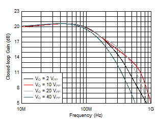
VO = 2 VPP
Figure 6-37 Small-Signal Frequency Response
GUID-9CDB22AC-0D3B-426D-BD3A-AD96983FE907-low.gif
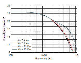
AV = 10 V/V
Figure 6-39 Large-Signal Frequency Response vs VO
GUID-EC7715E9-551D-43B0-97EF-9910D306174A-low.gif
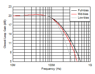
VO = 40 VPP
Figure 6-41 Large-Signal Frequency Response vs Bias Modes
GUID-3D9FA359-9CFD-4FDE-ACA7-139E257ACCF3-low.gif
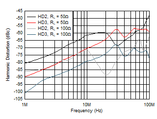
VO = 2 VPP
Figure 6-43 Harmonic Distortion vs Frequency
GUID-790E9D50-A549-4930-B3FE-469291F3C86E-low.gif
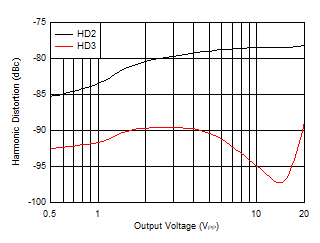
f = 1 MHz, RL = 50 Ω
Figure 6-45 Harmonic Distortion vs VO
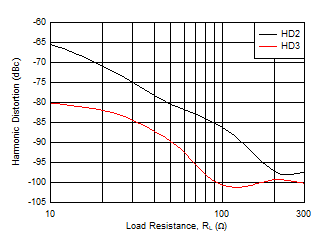
GUID-69C6F823-D468-4DFC-A6F6-36FA99EC4153-low.gif
f = 1 MHz, VO = 2 VPP
Figure 6-47 Harmonic Distortion vs RL
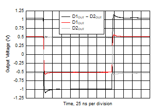
GUID-0BA507B4-07B1-44F3-A641-96229ED968E1-low.gif
VO step = 2 VPP
Figure 6-49 Small-Signal Pulse Response
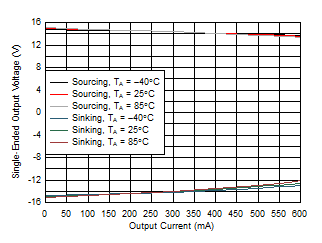
GUID-6AAC2D6F-B63F-4ADA-BA7B-850B2E92320C-low.gif
Average of 30 devices
Output voltage is slammed and IO is pulsed to maintain TJ as close to TA as possible.
Figure 6-51 Single-Ended Output Voltage vs IO and Temperature
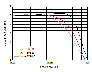
GUID-9FBE68BD-1FAA-455E-A8A0-D2A0C37A919A-low.gif
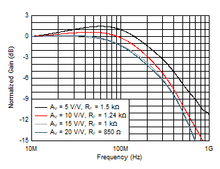
VO = 2 VPP
Figure 6-38 Small-Signal Frequency Response vs RF
GUID-30EAE7C4-7A79-4B08-86CD-750E8A5FA0D6-low.gif
AV = 15 V/V
Figure 6-40 Large-Signal Frequency Response vs VO
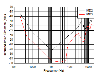
GUID-5EF51BB6-1A29-495E-9AD9-28EA69CA93EF-low.gif
Figure 6-42 Intermodulation Distortion vs Frequency
GUID-B7B66456-8547-44D5-9BF3-4C034011A652-low.gif
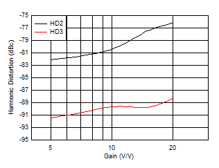
f = 1 MHz, VO = 2 VPP RL = 50 Ω
Figure 6-44 Harmonic Distortion vs Gain
GUID-8E74C289-45C6-4C68-BCB0-0EC59EF538D9-low.gif
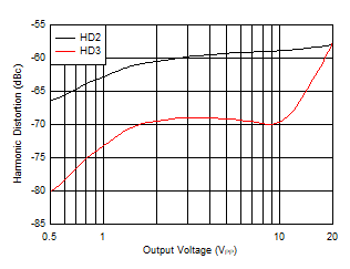
f = 10 MHz, RL = 50 Ω
Figure 6-46 Harmonic Distortion vs VO
GUID-677D8F5A-B5E3-4276-B145-D25373CB6B5A-low.gif
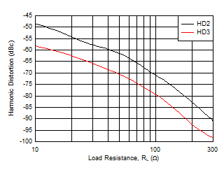
f = 10 MHz, VO = 2 VPP
Figure 6-48 Harmonic Distortion vs RL
GUID-FE6CAC2D-5A27-49F9-8810-3E39CD7A94B7-low.gif
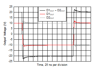
VO step = 40 VPP
Figure 6-50 Large-Signal Pulse Response
GUID-D6A07700-021B-4168-8B52-F209C284D11A-low.gif
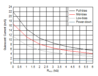
Average of 30 devices
Figure 6-52 Quiescent Current vs RADJ