ZHCSKA7F May 2019 – June 2021 LM61460-Q1
PRODUCTION DATA
- 1 特性
- 2 应用
- 3 说明
- 4 Revision History
- 5 Description (continued)
- 6 Device Comparison Table
- 7 Pin Configuration and Functions
- 8 Specifications
-
9 Detailed Description
- 9.1 Overview
- 9.2 Functional Block Diagram
- 9.3
Feature Description
- 9.3.1 EN/SYNC Uses for Enable and VIN UVLO
- 9.3.2 EN/SYNC Pin Uses for Synchronization
- 9.3.3 Clock Locking
- 9.3.4 Adjustable Switching Frequency
- 9.3.5 PGOOD Output Operation
- 9.3.6 Internal LDO, VCC UVLO, and BIAS Input
- 9.3.7 Bootstrap Voltage and VCBOOT-UVLO (CBOOT Pin)
- 9.3.8 Adjustable SW Node Slew Rate
- 9.3.9 Spread Spectrum
- 9.3.10 Soft Start and Recovery From Dropout
- 9.3.11 Output Voltage Setting
- 9.3.12 Overcurrent and Short Circuit Protection
- 9.3.13 Thermal Shutdown
- 9.3.14 Input Supply Current
- 9.4 Device Functional Modes
-
10Application and Implementation
- 10.1 Application Information
- 10.2
Typical Application
- 10.2.1 Design Requirements
- 10.2.2
Detailed Design Procedure
- 10.2.2.1 Choosing the Switching Frequency
- 10.2.2.2 Setting the Output Voltage
- 10.2.2.3 Inductor Selection
- 10.2.2.4 Output Capacitor Selection
- 10.2.2.5 Input Capacitor Selection
- 10.2.2.6 BOOT Capacitor
- 10.2.2.7 BOOT Resistor
- 10.2.2.8 VCC
- 10.2.2.9 BIAS
- 10.2.2.10 CFF and RFF Selection
- 10.2.2.11 External UVLO
- 10.2.3 Application Curves
- 11Power Supply Recommendations
- 12Layout
- 13Device and Documentation Support
- 14Mechanical, Packaging, and Orderable Information
8.8 Typical Characteristics
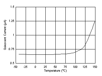
Unless otherwise specified, VIN = 13.5 V and fSW = 400 kHz.
| VFB = 1 V |
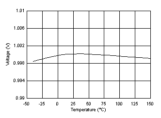
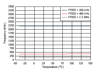 Figure 8-5 Switching Frequency Set by RT Resistor
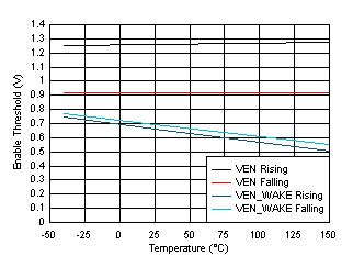 Figure 8-7 Enable Thresholds
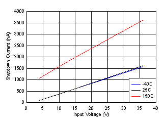
| VEN = 0 V |
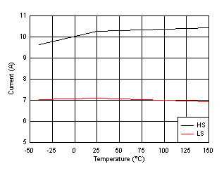 Figure 8-4 LM61460-Q1 High-side and Low-side Current Limits
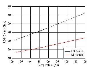 Figure 8-6 High-side and Low-side Switches RDS_ON
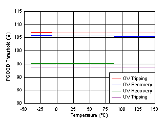 Figure 8-8 PGOOD Thresholds