ZHCSKB9Q December 1999 – October 2019 UCC1895 , UCC2895 , UCC3895
PRODUCTION DATA.
- 1 特性
- 2 应用
- 3 说明
- 4 修订历史记录
- 5 Pin Configuration and Functions
- 6 Specifications
-
7 Detailed Description
- 7.1 Overview
- 7.2 Functional Block Diagrams
- 7.3
Feature Description
- 7.3.1 ADS (Adaptive Delay Set)
- 7.3.2 CS (Current Sense)
- 7.3.3 CT (Oscillator Timing Capacitor)
- 7.3.4 DELAB and DELCD (Delay Programming Between Complementary Outputs)
- 7.3.5 EAOUT, EAP, and EAN (Error Amplifier)
- 7.3.6 OUTA, OUTB, OUTC, and OUTD (Output MOSFET Drivers)
- 7.3.7 PGND (Power Ground)
- 7.3.8 RAMP (Inverting Input of the PWM Comparator)
- 7.3.9 REF (Voltage Reference)
- 7.3.10 RT (Oscillator Timing Resistor)
- 7.3.11 GND (Analog Ground)
- 7.3.12 SS/DISB (Soft Start/Disable)
- 7.3.13 SYNC (Oscillator Synchronization)
- 7.3.14 VDD (Chip Supply)
- 7.4 Device Functional Modes
- 7.5 Programming
-
8 Application and Implementation
- 8.1 Application Information
- 8.2
Typical Application
- 8.2.1 Design Requirements
- 8.2.2
Detailed Design Procedure
- 8.2.2.1 Power Loss Budget
- 8.2.2.2 Preliminary Transformer Calculations (T1)
- 8.2.2.3 QA, QB, QC, QD FET Selection
- 8.2.2.4 Selecting LS
- 8.2.2.5 Selecting Diodes DB and DC
- 8.2.2.6 Output Inductor Selection (LOUT)
- 8.2.2.7 Output Capacitance (COUT)
- 8.2.2.8 Select Rectifier Diodes
- 8.2.2.9 Input Capacitance (CIN)
- 8.2.2.10 Current Sense Network (CT, RCS, RR, DA)
- 8.2.3 Application Curves
- 9 Power Supply Recommendations
- 10Layout
- 11器件和文档支持
- 12机械、封装和可订购信息
7.5.1 Programming DELAB, DELCD and the Adaptive Delay Set
The UCC3895 allows the user to set the delay between switch commands within each leg of the full-bridge power circuit according to Equation 5.

From Equation 5 VDEL is determined in conjunction with the desire to use (or not) the ADS feature from Equation 6.

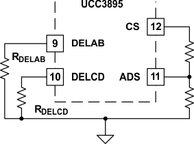
Figure 14 illustrates the resistors needed to program the delay periods and the ADS function.
 Figure 14. Programming Adaptive Delay Set
 The ADS allows the user to vary the delay times between switch commands within each of the two legs of the converter. The delay-time modulation is implemented by connecting ADS (pin 11) to CS, GND, or a resistive divider from CS through ADS to GND to set VADS as shown in Figure 14. From Equation 6 for VDEL, if ADS is tied to GND then VDEL rises in direct proportion to VCS, causing a decrease in tDELAY as the load increases. In this condition, the maximum value of VDEL is 2 V.
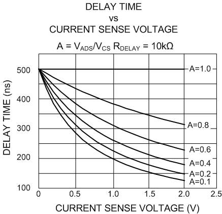
If ADS is connected to a resistive divider between CS and GND, the term (VCS – VADS) becomes smaller, reducing the level of VDEL. This reduction decreases the amount of delay modulation. In the limit of ADS tied to CS, VDEL = 0.5 V and no delay modulation occurs. Figure 15 graphically shows the delay time versus load for varying adaptive delay set feature voltages (VADS).
In the case of maximum delay modulation (ADS = GND), when the circuit goes from light load to heavy load, the variation of VDEL is from 0.5 to 2 V. This change causes the delay times to vary by a 4:1 ratio as the load is changed.
The ability to program an adaptive delay is a desirable feature because the optimum delay time is a function of the current flowing in the primary winding of the transformer, and changes by a factor of 10:1 or more as circuit loading changes. Reference 7 (see the 相关文档 section) describes the many interrelated factors for choosing the optimum delay times for the most efficient power conversion, and illustrates an external circuit to enable ADS using the UC3879. Implementing this adaptive feature is simplified in the UCC3895 controller, giving the user the ability to tailor the delay times to suit a particular application with a minimum of external parts.
 Figure 15. Delay Time Under Varying ADS Voltages