ZHCSKJ1A December 2019 – February 2020 TLV751
PRODUCTION DATA.
5 Pin Configuration and Functions
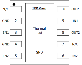
DSQ Package
10-Pin Adjustable WSON
Top View
DSQ Package
10-Pin Adjustable WSON
Top View

Pin Functions
| PIN | I/O | DESCRIPTION | |
|---|---|---|---|
| NAME | DSQ | ||
| EN1 | 3 | Input | Enable pin. Drive EN1 greater than VEN1(HI) to turn on the regulator.
Drive EN1 less than VEN1(LO) to put the low-dropout (LDO) regulator into shutdown mode. |
| EN2 | 5 | Input | Enable pin. Drive EN2 greater than VEN2(HI) to turn on the regulator.
Drive EN2 less than VEN2(LO) to put the LDO into shutdown mode. |
| FB1/ NC | 1 | — | For the adjustable TLV75101, this pin is used as an input to the control loop error amplifier and is used to set the output voltage of the LDO.
For the fixed TLV751xxxyyy, this is not connected internally. |
| FB2 / NC | 7 | — | For the adjustable TLV75101, this pin is used as an input to the control loop error amplifier and is used to set the output voltage of the LDO.
For the fixed TLV751xxxyyy, this is not connected internally. |
| GND | 2, 4 | — | Ground pin |
| IN1 | 9 | Input | Input pin. For best transient response and to minimize input impedance, use the recommended value or larger ceramic capacitor from IN to ground; see the Recommended Operating Conditions table and the Input and Output Capacitor Selection section. Place the input capacitor as close to the output of the device as possible. |
| IN2 | 6 | Input | Input pin. For best transient response and to minimize input impedance, use the recommended value or larger ceramic capacitor from IN to ground; see the Recommended Operating Conditions table and the Input and Output Capacitor Selection section. Place the input capacitor as close to the output of the device as possible. |
| OUT1 | 10 | Output | Regulated output voltage pin. A capacitor is required from OUT to ground for stability. For best transient response, use the nominal recommended value or larger ceramic capacitor from OUT to ground; see the Recommended Operating Conditions table and the Input and Output Capacitor Selection section. Place the output capacitor as close to output of the device as possible. |
| OUT2 | 8 | Output | Regulated output voltage pin. A capacitor is required from OUT to ground for stability. For best transient response, use the nominal recommended value or larger ceramic capacitor from OUT to ground; see the Recommended Operating Conditions table and the Input and Output Capacitor Selection section. Place the output capacitor as close to output of the device as possible. |
| Thermal pad | — | Connect the thermal pad to a large area GND plane for improved thermal performance. | |