ZHCSKO8C June 2021 – January 2022 UCC27614
PRODUCTION DATA
- 1 特性
- 2 应用
- 3 说明
- 4 Revision History
- 5 Pin Configuration and Functions
- 6 Specifications
- 7 Detailed Description
- 8 Applications and Implementation
- 9 Power Supply Recommendations
- 10Layout
- 11Device and Documentation Support
- 12Mechanical, Packaging, and Orderable Information
7.3.4 Output Stage
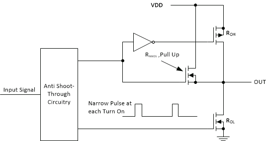
The output stage of the UCC27614 device is illustrated in Figure 7-2. The UCC27614 device features a unique architecture on the output stage which delivers the highest peak source current when it is most needed during the Miller plateau region of the power switch turnon transition (when the power switch drain/collector voltage experiences dV/dt). The device output stage features a hybrid pullup structure using a parallel arrangement of N-Channel and P-Channel MOSFET devices. By turning on the N-Channel MOSFET during a narrow instant when the output changes state from low to high, the gate driver device is able to deliver a brief boost in the peak sourcing current enabling fast turnon. The on-resistance of this N-channel MOSFET (RNMOS) is approximately 0.52 Ω when activated.
 Figure 7-2 UCC27614
Gate Driver Output Stage
Figure 7-2 UCC27614
Gate Driver Output StageThe ROH parameter (see Electrical Table) is a DC measurement and it is representative of the on-resistance of the P-Channel device only, because the N-Channel device is turned on only during output change of state from low to high. Thus, the effective resistance of the hybrid pullup stage is much lower than what is represented by ROH parameter. The pulldown structure is composed of a N-channel MOSFET only. The ROL is also a DC measurement, and it is representative of true impedance of the pulldown stage in the device.
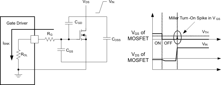
The UCC27614 can deliver 10-A source, and up to 10-A sink at VDD = 12 V. Strong sink capability results in a very low pulldown impedance in the driver output stage which boosts immunity against the parasitic Miller turnon (high slew rate dV/dt turnon) effect that is seen in both IGBT and FET power switches.
An example of a situation where Miller turnon is a concern is synchronous rectification (SR). In SR application, the dV/dt occurs on MOSFET drain when the MOSFET is already held in OFF state by the gate driver. The current charging the CGD Miller capacitance during this high dV/dt is shunted by the pulldown stage of the driver. If the pulldown impedance is not low enough then a voltage spike can result in the VGS of the MOSFET, which can result in spurious turnon. This phenomenon is illustrated in Figure 7-3.
 Figure 7-3 Low Pull-Down Impedance in UCC27614 (Output Stage Mitigates Miller Turnon Effect)
The driver output voltage swings between VDD and GND providing rail-to-rail operation because of the low dropout of the output stage. In most applications, the external Schottky diode clamps may be eliminated because the presence of the MOSFET body diodes offers low impedance to switching overshoots and undershoots. The output stage of the UCC27614 devices can handle significant transient reverse current. The two OUT pins of the device should be shorted on the application board. The application may use resistor and parallel diode-resistor combination at the gate of the MOSFET or IGBT to program different rise (pullup current) time and fall (pulldown) time.