ZHCSKU9B February 2020 – October 2024 ADC09DJ1300-Q1 , ADC09QJ1300-Q1 , ADC09SJ1300-Q1
PRODUCTION DATA
- 1
- 1 特性
- 2 应用
- 3 说明
- 4 Pin Configuration and Functions
-
5 Specifications
- 5.1 Absolute Maximum Ratings
- 5.2 ESD Ratings
- 5.3 Recommended Operating Conditions
- 5.4 Thermal Information
- 5.5 Electrical Characteristics: DC Specifications
- 5.6 Electrical Characteristics: Power Consumption
- 5.7 Electrical Characteristics: AC Specifications
- 5.8 Timing Requirements
- 5.9 Switching Characteristics
- 5.10 Typical Characteristics
-
6 Detailed Description
- 6.1 Overview
- 6.2 Functional Block Diagram
- 6.3
Feature Description
- 6.3.1 Device Comparison
- 6.3.2
Analog Input
- 6.3.2.1 Analog Input Protection
- 6.3.2.2 Full-Scale Voltage (VFS) Adjustment
- 6.3.2.3 Analog Input Offset Adjust
- 6.3.2.4 ADC Core
- 6.3.2.5 Temperature Monitoring Diode
- 6.3.2.6 Timestamp
- 6.3.2.7 Clocking
- 6.3.2.8
JESD204C Interface
- 6.3.2.8.1 Transport Layer
- 6.3.2.8.2 Scrambler
- 6.3.2.8.3 Link Layer
- 6.3.2.8.4 8B/10B Link Layer
- 6.3.2.8.5 64B/66B Link Layer
- 6.3.2.8.6 Physical Layer
- 6.3.2.8.7 JESD204C Enable
- 6.3.2.8.8 Multi-Device Synchronization and Deterministic Latency
- 6.3.2.8.9 Operation in Subclass 0 Systems
- 6.3.2.8.10 Alarm Monitoring
- 6.4
Device Functional Modes
- 6.4.1 Low Power Mode and High Performance Mode
- 6.4.2 JESD204C Modes
- 6.4.3 Power-Down Modes
- 6.4.4
Test Modes
- 6.4.4.1 Serializer Test-Mode Details
- 6.4.4.2 PRBS Test Modes
- 6.4.4.3 Clock Pattern Mode
- 6.4.4.4 Ramp Test Mode
- 6.4.4.5 Short and Long Transport Test Mode
- 6.4.4.6 D21.5 Test Mode
- 6.4.4.7 K28.5 Test Mode
- 6.4.4.8 Repeated ILA Test Mode
- 6.4.4.9 Modified RPAT Test Mode
- 6.4.4.10 Calibration Modes and Trimming
- 6.4.4.11 Offset Calibration
- 6.4.4.12 Trimming
- 6.5 Programming
- 6.6 SPI_Register_Map Registers
- 7 Application and Implementation
- 8 Device and Documentation Support
- 9 Revision History
- 10Mechanical, Packaging, and Orderable Information
6.4.1 Low Power Mode and High Performance Mode
Device power consumption can be reduced at the tradeoff of performance by programming the device into the Low Power Mode. This mode is only available when operating at 1 GSPS or less and is recommended to only be used for 1st Nyquist zone applications. The default operating mode is High Performance Mode which is enabled by the default register values. Table 6-13 shows the register writes to switch between the lowest power configuration of Low Power Mode and High Performance Mode. These writes should only be performed when CAL_EN is set to 0 and JESD_EN is set to 0.
| Register Name (Address) | Low Power Mode Value | High Performance Mode Value (Default Mode) |
|---|---|---|
| LOW_POWER1 (0x037) | 0x46 | 0x4B |
| LOW_POWER2 (0x29A) | 0x06 | 0x0F |
| LOW_POWER3 (0x29B) | 0x00 | 0x04 |
| LOW_POWER4 (0x29C) | 0x14 | 0x1B |
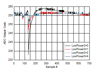
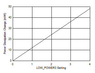
The magnitude of the glitch during the transition between ADC cores during background calibration and low power background calibration is affected by the setting of the LOW_POWER3 register setting (Address = 0x29B). A lower power can be traded off vs larger glitch magnitude. The ADC output during the transition between ADC cores for low power mode is shown in Figure 6-12 and the power dissipation change vs LOW_POWER3 setting is shown in Figure 6-13. A setting of 4 reduces the glitch to the same magnitude as high performance mode.
 Figure 6-12 Background Calibration Core Transition In Low Power Mode
 Figure 6-13 Power
Dissipation Change vs LOW_POWER3 register setting
Figure 6-13 Power
Dissipation Change vs LOW_POWER3 register settingIn low power background calibration mode, the timing of the ADC transition can be controlled by setting register LP_TRIG = 1. The ADC transition will occur in the ADC output data between 500 and 1000 ADC sample clocks after triggering by the CALTRIG ball or SPI write to CAL_SOFT_TRIG register (Address = 0x6C).
Foreground calibration mode has no ADC core transitions and no glitch.