ZHCSL06D February 2008 – February 2020 TPS51200
PRODUCTION DATA.
- 1 特性
- 2 应用
- 3 说明
- 4 修订历史记录
- 5 Pin Configuration and Functions
- 6 Specifications
-
7 Detailed Description
- 7.1 Overview
- 7.2 Functional Block Diagram
- 7.3
Feature Description
- 7.3.1 Sink and Source Regulator (VO Pin)
- 7.3.2 Reference Input (REFIN Pin)
- 7.3.3 Reference Output (REFOUT Pin)
- 7.3.4 Soft-Start Sequencing
- 7.3.5 Enable Control (EN Pin)
- 7.3.6 Powergood Function (PGOOD Pin)
- 7.3.7 Current Protection (VO Pin)
- 7.3.8 UVLO Protection (VIN Pin)
- 7.3.9 Thermal Shutdown
- 7.3.10 Tracking Start-up and Shutdown
- 7.3.11 Output Tolerance Consideration for VTT DIMM Applications
- 7.3.12 REFOUT (VREF) Consideration for DDR2 Applications
- 7.4 Device Functional Modes
- 8 Application and Implementation
- 9 Power Supply Recommendations
- 10Layout
- 11器件和文档支持
- 12机械、封装和可订购信息
7.3.12 REFOUT (VREF) Consideration for DDR2 Applications
During TPS51200 tracking start-up, the REFIN voltage follows the rise of the VDDQ rail through a voltage divider, and REFOUT (VREF) follows REFIN once the REFIN voltage is greater than 0.39 V. When the REFIN voltage is lower than 0.39 V, VREF is 0 V.
The JEDEC DDR2 SDRAM Standard (JESD79-2E) states that VREF must track VDDQ/2 within ±0.3 V accuracy during the start-up period. To allow the TPS51200
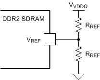
device to meet the JEDEC DDR2 specification, a resistor divider can be used to provide the VREF signal to the DIMM. The resistor divider ratio is 0.5 to ensure that the VREF voltage equals VDDQ/2.
 Figure 23. Resistor Divider Circuit
 When selecting the resistor value, consider the impact of the leakage current from the DIMM VREF pin on the reference voltage. Use Equation 4 to calculate resistor values.

where
- RREF is the resistor value
- ∆VREF is the VREF DC variation requirement
- IREF is the maximum total VREF leakage current from DIMMs
Consider the MT47H64M16 DDR2 SDRAM component from Micron as an example. The MT47H64M16 datasheet shows the maximum VREF leakage current of each DIMM is ±2 µA, and VREF(DC) variation must be within ±1% of VDDQ. In this DDR2 application, the VDDQ voltage is 1.8 V. Assuming one TPS51200 device needs to power 4 DIMMs, the maximum total VREF leakage current is ±8 µA. Based on the calculations, the resistor value should be lower than 4.5 kΩ. To ensure sufficient margin, 100 Ω is the suggested resistor value. With two 100-Ω resistors, the maximum VREF variation is 0.4 mV, and the power loss on each resistor is 8.1 mW.