ZHCSL06D February 2008 – February 2020 TPS51200
PRODUCTION DATA.
- 1 特性
- 2 应用
- 3 说明
- 4 修订历史记录
- 5 Pin Configuration and Functions
- 6 Specifications
-
7 Detailed Description
- 7.1 Overview
- 7.2 Functional Block Diagram
- 7.3
Feature Description
- 7.3.1 Sink and Source Regulator (VO Pin)
- 7.3.2 Reference Input (REFIN Pin)
- 7.3.3 Reference Output (REFOUT Pin)
- 7.3.4 Soft-Start Sequencing
- 7.3.5 Enable Control (EN Pin)
- 7.3.6 Powergood Function (PGOOD Pin)
- 7.3.7 Current Protection (VO Pin)
- 7.3.8 UVLO Protection (VIN Pin)
- 7.3.9 Thermal Shutdown
- 7.3.10 Tracking Start-up and Shutdown
- 7.3.11 Output Tolerance Consideration for VTT DIMM Applications
- 7.3.12 REFOUT (VREF) Consideration for DDR2 Applications
- 7.4 Device Functional Modes
- 8 Application and Implementation
- 9 Power Supply Recommendations
- 10Layout
- 11器件和文档支持
- 12机械、封装和可订购信息
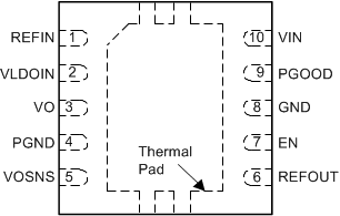
5 Pin Configuration and Functions
DRC Package
10-Pin VSON
Top View

Pin Functions
| PIN | I/O(2) | DESCRIPTION | |
|---|---|---|---|
| NAME | NO. | ||
| EN | 7 | I | For DDR VTT application, connect EN to SLP_S3. For any other application, use the EN pin as the ON/OFF function. |
| GND | 8 | G | Signal ground. |
| PGND(1) | 4 | G | Power ground for the LDO. |
| PGOOD | 9 | O | Open-drain, power-good indicator. |
| REFIN | 1 | I | Reference input. |
| REFOUT | 6 | O | Reference output. Connect to GND through 0.1-μF ceramic capacitor. If there is a REFOUT capacitors at DDR side, keep total capacitance on REFOUT pin below 0.47 μF. The REFOUT pin can not be open. |
| VIN | 10 | I | 2.5-V or 3.3-V power supply. A ceramic decoupling capacitor with a value between 1-μF and 4.7-μF is required. |
| VLDOIN | 2 | I | Supply voltage for the LDO. |
| VO | 3 | O | Power output for the LDO. |
| VOSNS | 5 | I | Voltage sense input for the LDO. Connect to positive terminal of the output capacitor or the load. |
(1) Thermal pad connection. See Figure 35 in the Thermal Design Considerations section for additional information.
(2) I = Input, O = Output , G = Ground