at TA = 25°C, VIN = 1.4 V or
VIN = VOUT(nom) + 0.4 V (whichever is greater),
VBIAS = open, VOUT(nom) = 0.5 V, VEN = 1.1 V,
CIN = 10 μF, COUT = 47 μF, CNR/SS = 0 nF, no
CFF, and PG pin pulled up to VIN with 100 kΩ (unless
otherwise noted)

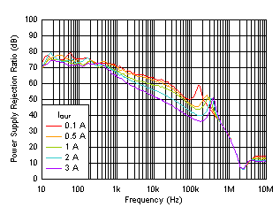
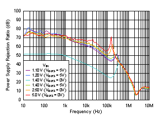
VIN = 1.1 V, VBIAS = 5 V,
COUT = 47 μF || 10 μF || 10 μF,
CNR/SS = 10 nF,
CFF = 10 nF |
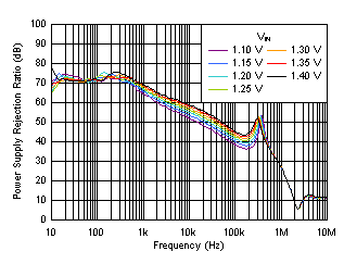
Figure 6-43 PSRR
vs Frequency and IOUT
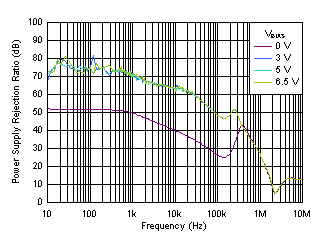
VIN = 1.4 V, IOUT = 1 A,
COUT = 47 μF || 10 μF || 10 μF,
CNR/SS = 10 nF,
CFF = 10 nF |
Figure 6-45 PSRR
vs Frequency and VBIAS
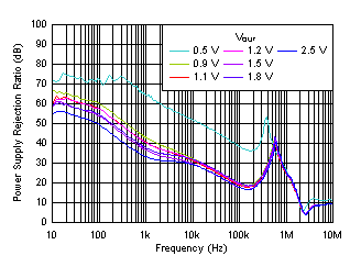
VIN = VOUT + 0.3 V or
VIN = 1.1 V (whichever is greater),
VBIAS = 5 V, IOUT = 3 A,
COUT = 47 μF || 10 μF || 10 μF,
CNR/SS = 10 nF,
CFF = 10 nF |
Figure 6-47 PSRR
vs Frequency and VOUT With Bias
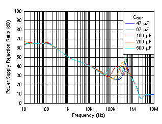
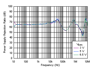
VIN = 1.4 V, VBIAS = 5 V,
VOUT = 1 V, IOUT = 3 A,
CNR/SS = 10 nF,
CFF = 10 nF |
Figure 6-49 PSRR
vs Frequency and COUT
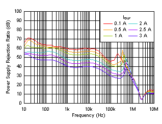
| VIN = 5.5 V, VOUT = 5 V,
IOUT = 3 A, COUT = 47 μF || 10
μF || 10 μF, CNR/SS = 10 nF, CFF =
10 nF |
Figure 6-51 PSRR
vs Frequency and IOUT
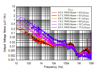
(VOUT = 5 V)
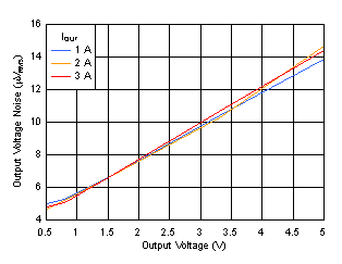
| VIN = VOUT + 0.3 V or
VIN = 1.1 V (whichever is greater),
VBIAS = 5 V for VIN ≤ 2.2 V,
COUT = 47 μF || 10 μF || 10 μF,
CNR/SS = 10 nF, CFF = 10 nF,
RMS noise BW = 10 Hz to 100 kHz |
| |
Figure 6-53 Output Voltage Noise vs VOUT
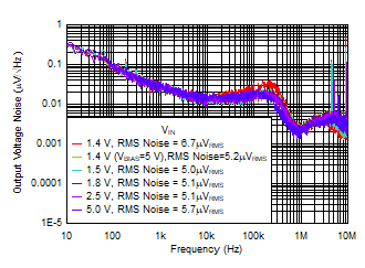
| VOUT = 0.7 V, IOUT = 3 A,
COUT = 47 μF || 10 μF || 10 μF,
CNR/SS = 10 nF, CFF = 10 nF,
RMS noise BW = 10 Hz to 100 kHz |
Figure 6-55 Output Noise vs Frequency and VIN
| VOUT = 0.7 V, VIN = 1.1 V,
VBIAS = 5 V, IOUT = 3 A,
COUT = 47 μF || 10 μF || 10 μF,
CNR/SS = 10 nF, RMS noise BW = 10 Hz to
100 kHz |
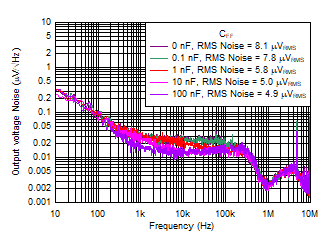
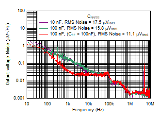
Figure 6-57 Output Noise vs Frequency and CFF
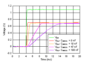
VIN = 1.2 V, VOUT = 0.7 V,
VBIAS = 5 V, IOUT = 3 A,
COUT = 47 μF ||
10 μF || 10 μF, CFF = 10 nF |
| |
Figure 6-59 Start-Up Waveform vs Time and CNR/SS
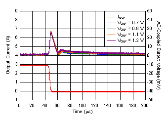
VIN = VOUT + 0.5 V,
VBIAS = 5 V, IOUT = 3 A to 100
mA,
slew rate = 1 A/μs,
CNR/SS = CFF = 10 nF,
COUT = 47 μF ||
10 μF || 10 μF |
Figure 6-61 Load
Transient vs Time and VOUT With Bias
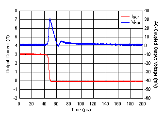
VIN = VOUT + 0.5 V,
VOUT = 0.7 V, IOUT = 3 A to
100 mA,
COUT =
47 μF || 10 μF || 10 μF, CNR/SS =
CFF = 10 nF, slew rate = 1 A/μs |
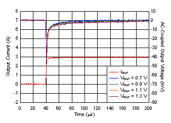
Figure 6-63 Load
Transient vs Time and VOUT Without Bias
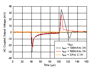
VIN = 1.2 V, VOUT = 0.7 V,
VBIAS = 5 V, slew rate = 1 A/μs,
COUT = 47 μF ||
10 μF || 10 μF, CNR/SS = CFF = 10
nF |
Figure 6-65 Load
Transient vs Time and DC Load
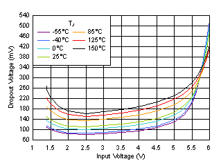
| IOUT = 3 A, VBIAS = 5.0
V |
Figure 6-67 Dropout Voltage vs VIN With Bias
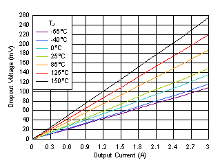
| VIN = 1.1 V, VBIAS = 5.0
V |
Figure 6-69 Dropout Voltage vs IOUT With Bias Figure 6-71 Load
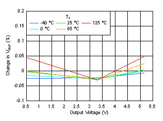
Regulation vs VOUT
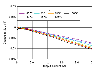
 Figure 6-73 Load
Regulation vs IOUT (3.3-V Output)
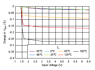
| VOUT = 0.5 V, IOUT = 5
mA |
Figure 6-75 Line
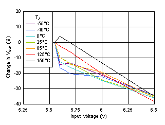
Regulation vs VIN Figure 6-77 Line
Regulation vs VIN (5.15-V Output)
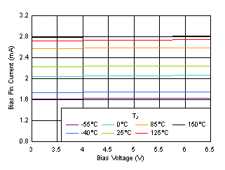
 Figure 6-79 Bias
Pin Current With Bias
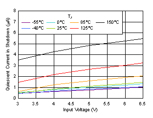
 Figure 6-81 Shutdown Current vs VIN With Bias
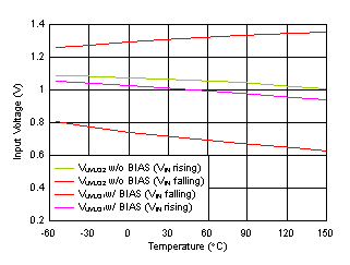
 Figure 6-83 VIN UVLO vs Temperature
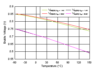
 Figure 6-85 Enable Threshold vs Temperature
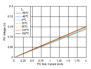
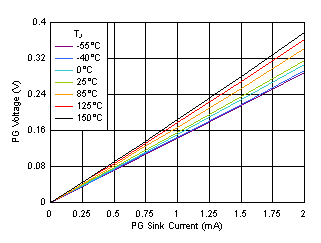
 Figure 6-87 PG
Voltage vs PG Current Sink
IOUT = 3 A, VBIAS = 5 V,
COUT = 47 μF || 10 μF || 10 μF,
CNR/SS = 10 nF,
CFF = 10 nF |
Figure 6-44 PSRR
vs Frequency and VIN With Bias
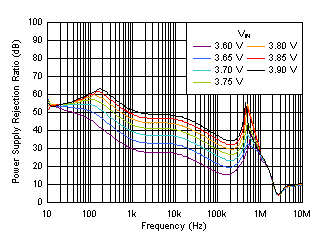
IOUT = 1 A, COUT = 47 μF ||
10 μF || 10 μF, CNR/SS = 10 nF,
CFF = 10
nF |
Figure 6-46 PSRR
vs Frequency and VIN
IOUT = 3 A, COUT = 47 μF ||
10 μF || 10 μF, CNR/SS = 10 nF,
CFF = 10
nF |
| |
Figure 6-48 PSRR
vs Frequency and VIN
(VOUT = 3.3 V)
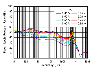
VOUT = 5 V, IOUT = 3 A,
COUT = 47 μF || 10 μF || 10 μF,
CNR/SS = 10 nF,
CFF = 10 nF |
Figure 6-50 PSRR
vs Frequency and VIN
(VOUT = 5 V)
| VIN = VOUT + 0.3 V,
VOUT = 1 V, IOUT = 3 A,
COUT = 47 μF || 10 μF || 10 μF,
CNR/SS = 10 nF, CFF = 10
nF |
Figure 6-52 VBIAS PSRR vs Frequency
| VIN = VOUT + 0.3 V or
VIN = 1.1 V (whichever is greater),
VBIAS = 5 V for VIN ≤ 2.2 V,
IOUT = 3 A, COUT = 47 μF || 10
μF || 10 μF, CNR/SS = 10 nF, CFF =
10 nF, RMS noise BW = 10 Hz to 100 kHz |
Figure 6-54 Output Noise vs Frequency and VOUT
| VOUT = 0.7 V, VIN = 1.1 V,
VBIAS = 5 V, IOUT = 3 A,
COUT = 47 μF || 10 μF || 10 μF,
CFF = 10 nF, RMS noise BW = 10 Hz to 100
kHz |
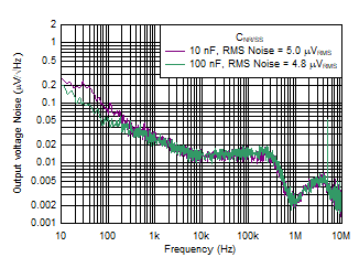
Figure 6-56 Output Noise vs Frequency and CNR/SS
| VIN = VOUT + 0.3 V,
VBIAS = 5 V, IOUT = 3 A,
COUT = 47 μF || 10 μF || 10 μF,
CFF = 10 nF, RMS noise BW = 10 Hz to 100
kHz |
Figure 6-58 Output Noise vs Frequency
(5-V
Output)
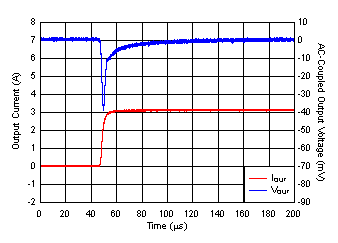
VIN = VOUT + 0.5 V,
VBIAS = 5 V, IOUT = 100 mA to
3 A,
slew rate = 1 A/μs,
CNR/SS = CFF = 10 nF,
COUT = 47 μF ||
10 μF || 10 μF |
Figure 6-60 Load
Transient vs Time and VOUT With Bias
VIN = VOUT + 0.5 V,
VOUT = 0.7 V, IOUT = 100 mA to
3 A,
COUT = 47
μF || 10 μF || 10 μF, CNR/SS = CFF
= 10 nF, slew rate = 1 A/μs |
Figure 6-62 Load
Transient vs Time and VOUT Without Bias
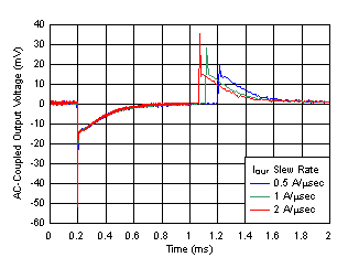
VOUT = 5 V, IOUT, DC = 100
mA, IOUT = 100 mA to 3 A,
COUT = 47 μF ||
10 μF || 10 μF, CNR/SS = CFF = 10
nF |
Figure 6-64 Load
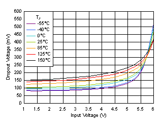
Transient vs Time and Slew Rate Figure 6-66 Dropout Voltage vs VIN Without Bias
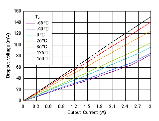
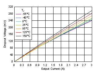
 Figure 6-68 Dropout Voltage vs IOUT Without Bias
 Figure 6-70 Dropout Voltage vs IOUT (High VIN)
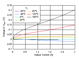
 Figure 6-72 Load
Regulation vs IOUT
| VIN = 5.55 V, VOUT = 5.15
V |
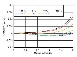
Figure 6-74 Load
Regulation vs IOUT (5-V Output)
| VOUT = 0.5 V, VIN = 1.1 V,
IOUT = 5 mA |
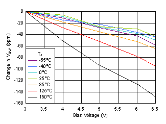
Figure 6-76 Line
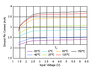
Regulation With Bias Figure 6-78 Ground Pin Current vs VIN
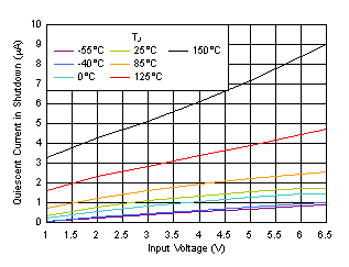
 Figure 6-80 Shutdown Current vs VIN
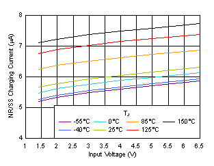
 Figure 6-82 INR/SS Current vs VIN
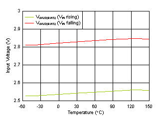
 Figure 6-84 VBIAS UVLO vs Temperature
 Figure 6-86 PG
Voltage vs PG Current Sink
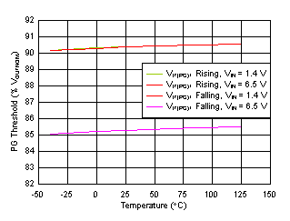
 Figure 6-88 PG
Threshold vs Temperature