ZHCSL68C April 2017 – December 2020 TPS7A84A
PRODUCTION DATA
- 1 特性
- 2 应用
- 3 说明
- 4 Revision History
- 5 Pin Configuration and Functions
-
6 Specifications
- 6.1 Absolute Maximum Ratings
- 6.2 ESD Ratings
- 6.3 Recommended Operating Conditions
- 6.4 Thermal Information
- 6.5 Electrical Characteristics: General
- 6.6 Electrical Characteristics: TPS7A8400A
- 6.7 Electrical Characteristics: TPS7A8401A
- 6.8 Typical Characteristics: TPS7A8400A
- 6.9 Typical Characteristics: TPS7A8401A
- 7 Detailed Description
-
8 Application and Implementation
- 8.1
Application Information
- 8.1.1
External Component Selection
- 8.1.1.1 Adjustable Operation
- 8.1.1.2 ANY-OUT Programmable Output Voltage
- 8.1.1.3 ANY-OUT Operation
- 8.1.1.4 Increasing ANY-OUT Resolution for LILO Conditions
- 8.1.1.5 Current Sharing
- 8.1.1.6 Recommended Capacitor Types
- 8.1.1.7 Input and Output Capacitor Requirements (CIN and COUT)
- 8.1.1.8 Feed-Forward Capacitor (CFF)
- 8.1.1.9 Noise-Reduction and Soft-Start Capacitor (CNR/SS)
- 8.1.2 Start-Up
- 8.1.3 AC and Transient Performance
- 8.1.4 DC Performance
- 8.1.5 Sequencing Requirements
- 8.1.6 Negatively Biased Output
- 8.1.7 Reverse Current Protection
- 8.1.8 Power Dissipation (PD)
- 8.1.1
External Component Selection
- 8.2 Typical Applications
- 8.1
Application Information
- 9 Power Supply Recommendations
- 10Layout
- 11Device and Documentation Support
8.1.3.3.1 Charge Pump Noise
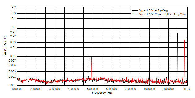
The device internal charge pump generates a minimal amount of noise, as shown in Figure 8-8.
Using a bias rail minimizes the internal charge-pump noise when the internal voltage is clamped, thereby reducing the overall output noise floor.
The high-frequency components of the output voltage noise density curve are filtered out in most applications by using 10-nF to 100-nF bypass capacitors close to the load. Using a ferrite bead between the LDO output and the load input capacitors forms a pi-filter, further reducing the high-frequency noise contribution.
 Figure 8-8 Charge Pump Noise