ZHCSL85B May 2020 – April 2021 AMC3306M25
PRODUCTION DATA
- 1 特性
- 2 应用
- 3 说明
- 4 Revision History
- 5 Pin Configuration and Functions
-
6 Specifications
- 6.1 Absolute Maximum Ratings
- 6.2 ESD Ratings
- 6.3 Recommended Operating Conditions
- 6.4 Thermal Information
- 6.5 Power Ratings
- 6.6 Insulation Specifications
- 6.7 Safety-Related Certifications
- 6.8 Safety Limiting Values
- 6.9 Electrical Characteristics
- 6.10 Switching Characteristics
- 6.11 Timing Diagrams
- 6.12 Insulation Characteristics Curves
- 6.13 Typical Characteristics
- 7 Detailed Description
- 8 Application and Implementation
- 9 Power Supply Recommendations
- 10Layout
- 11Device and Documentation Support
- 12Mechanical, Packaging, and Orderable Information
7.3.3 Isolation Channel Signal Transmission
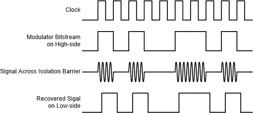
The AMC3306M25 uses an on-off keying (OOK) modulation scheme, as shown in Figure 7-3, to transmit the modulator output bitstream across the SiO2-based isolation barrier. The transmit driver (TX) illustrated in the Section 7.2 transmits an internally generated, high-frequency carrier across the isolation barrier to represent a digital one and does not send a signal to represent a digital zero. The nominal frequency of the carrier used inside the AMC3306M25 is 480 MHz.
Figure 7-3 shows the concept of the on-off keying scheme.
 Figure 7-3 OOK-Based
Modulation Scheme