ZHCSLA3A May 2020 – December 2020 LM7481-Q1
PRODUCTION DATA
- 1 特性
- 2 应用
- 3 说明
- 4 Revision History
- 5 Pin Configuration and Functions
- 6 Specifications
- 7 Parameter Measurement Information
- 8 Detailed Description
-
9 Application and Implementation
- 9.1 Application Information
- 9.2
Typical 12-V Reverse Battery Protection Application
- 9.2.1 Design Requirements for 12-V Battery Protection
- 9.2.2 Automotive Reverse Battery Protection
- 9.2.3 Input Transient Protection: ISO 7637-2 Pulse 1
- 9.2.4 AC Super Imposed Input Rectification: ISO 16750-2 and LV124 E-06
- 9.2.5 Input Micro-Short Protection: LV124 E-10
- 9.2.6 Detailed Design Procedure
- 9.2.7 MOSFET Selection: Blocking MOSFET Q1
- 9.2.8 MOSFET Selection: Hot-Swap MOSFET Q2
- 9.2.9 TVS selection
- 9.2.10 Application Curves
- 9.3 Do's and Don'ts
- 10Power Supply Recommendations
- 11Layout
- 12Device and Documentation Support
- 13Mechanical, Packaging, and Orderable Information
9.2.10 Application Curves
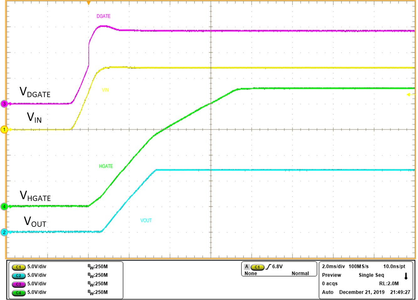 Figure 9-7 Startup 12 V with EN pulled to VIN
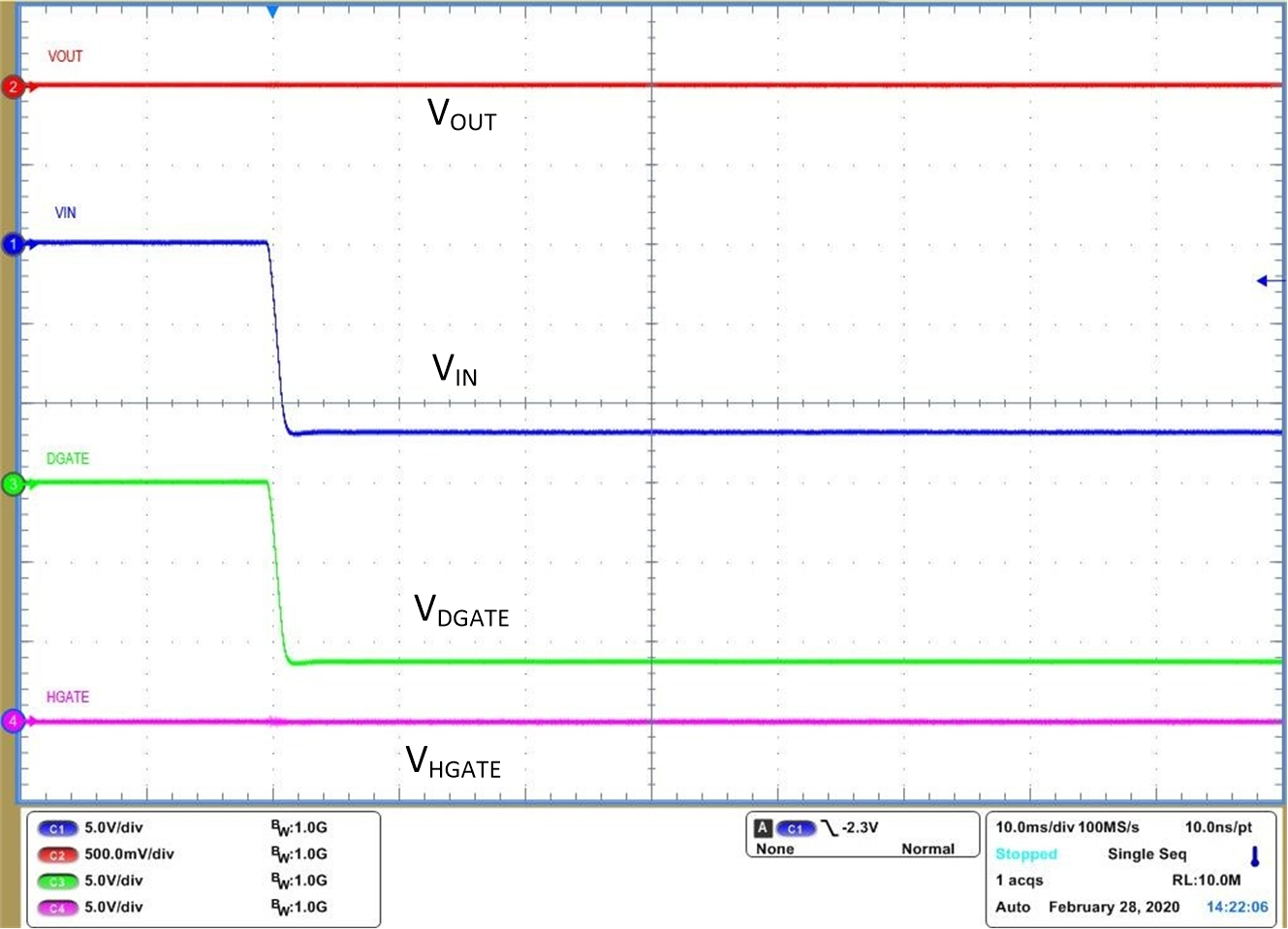 Figure 9-9 Reverse Input Voltage -12 V
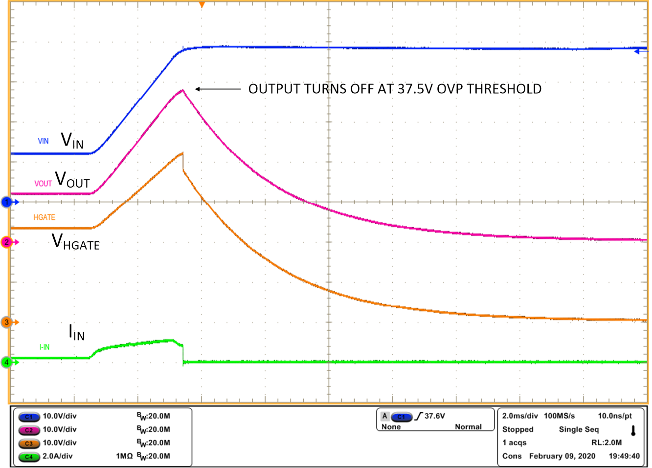 Figure 9-11 Over Voltage Cut-off
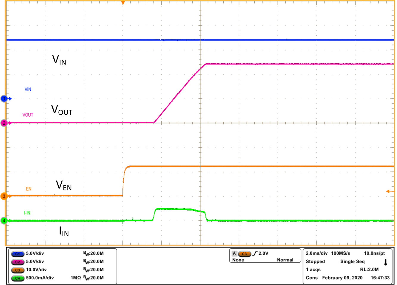 Figure 9-13 Turn ON with ENABLE Control
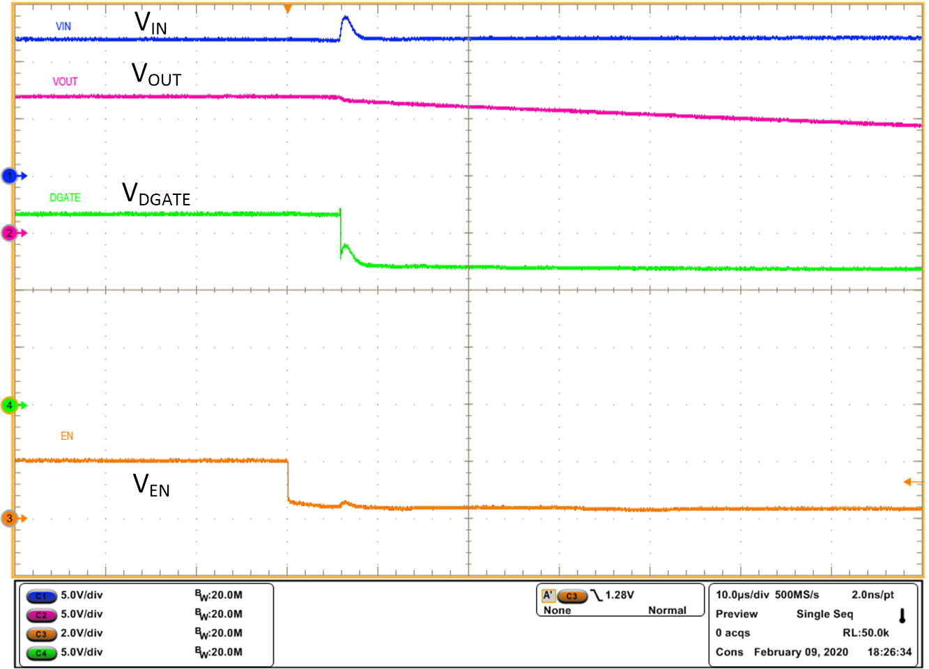 Figure 9-15 Disable Delay DGATE
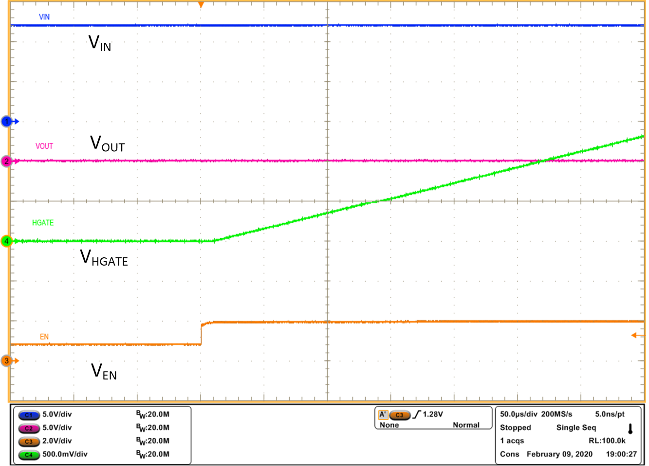 Figure 9-17 Enable Delay HGATE
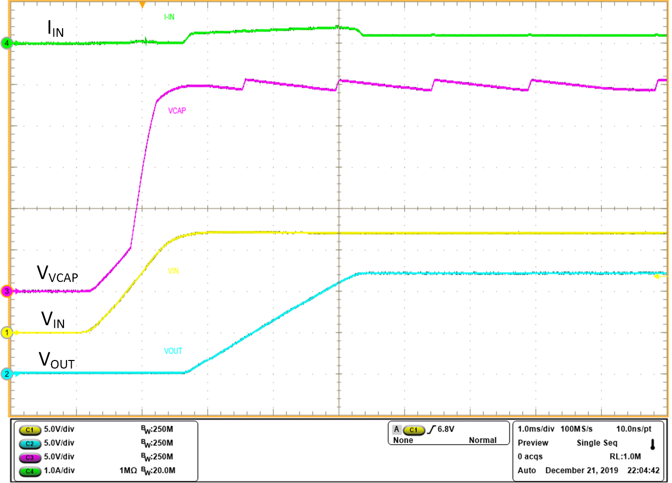 Figure 9-8 Startup 12 V showing Charge Pump VCAP
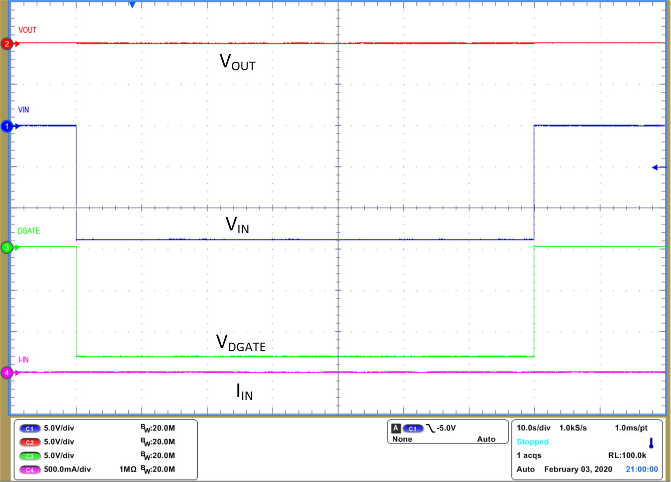 Figure 9-10 Reverse Input Voltage -12 V for 60s
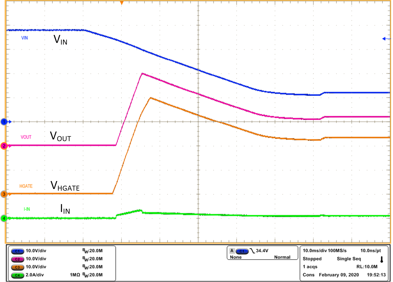 Figure 9-12 Over Voltage Recovery
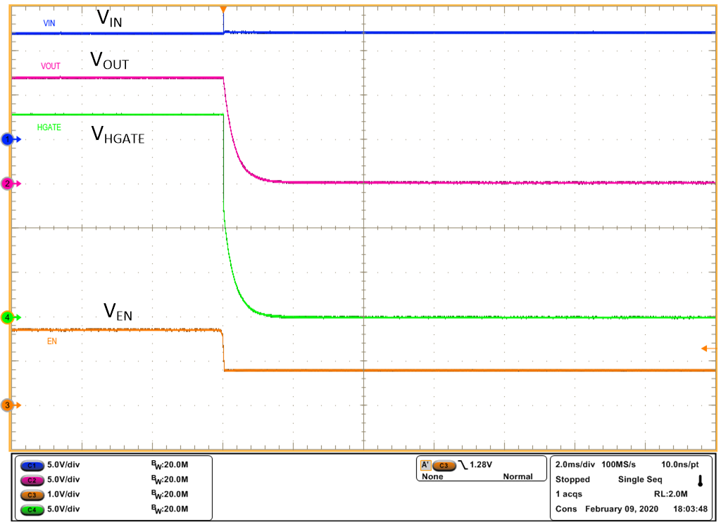 Figure 9-14 Turn OFF with ENABLE Control
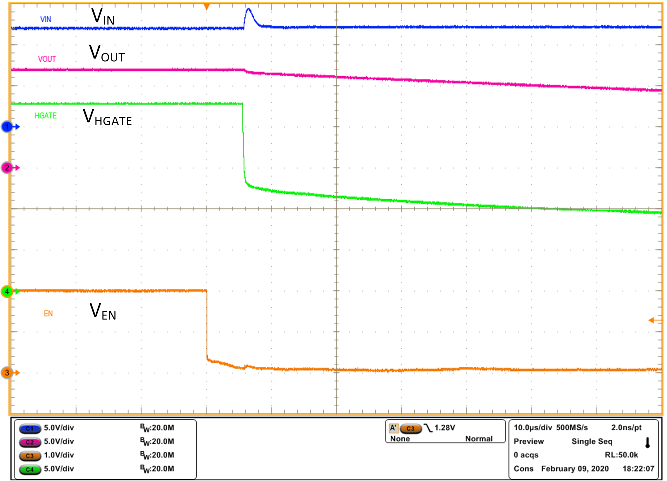 Figure 9-16 Disable Delay HGATE
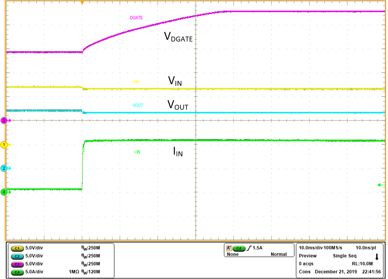 Figure 9-18 Load Transient Response DGATE