ZHCSLA3A May 2020 – December 2020 LM7481-Q1
PRODUCTION DATA
- 1 特性
- 2 应用
- 3 说明
- 4 Revision History
- 5 Pin Configuration and Functions
- 6 Specifications
- 7 Parameter Measurement Information
- 8 Detailed Description
-
9 Application and Implementation
- 9.1 Application Information
- 9.2
Typical 12-V Reverse Battery Protection Application
- 9.2.1 Design Requirements for 12-V Battery Protection
- 9.2.2 Automotive Reverse Battery Protection
- 9.2.3 Input Transient Protection: ISO 7637-2 Pulse 1
- 9.2.4 AC Super Imposed Input Rectification: ISO 16750-2 and LV124 E-06
- 9.2.5 Input Micro-Short Protection: LV124 E-10
- 9.2.6 Detailed Design Procedure
- 9.2.7 MOSFET Selection: Blocking MOSFET Q1
- 9.2.8 MOSFET Selection: Hot-Swap MOSFET Q2
- 9.2.9 TVS selection
- 9.2.10 Application Curves
- 9.3 Do's and Don'ts
- 10Power Supply Recommendations
- 11Layout
- 12Device and Documentation Support
- 13Mechanical, Packaging, and Orderable Information
9.2.4 AC Super Imposed Input Rectification: ISO 16750-2 and LV124 E-06
Alternators are used to power the automotive electrical system and charge the battery during normal runtime of the vehicle. Rectified alternator output contains residual AC ripple voltage superimposed on the DC battery voltage due to various reasons which includes engine speed variation, regulator duty cycle with field switching ON/OFF and electrical load variations. On a 12-V battery supply, alternator output voltage is regulated by a voltage regulator between 14.5 V to 12.5 V by controlling the field current of alternator's rotor. All electronic modules are tested for proper operation with superimposed AC ripple on the DC battery voltage. AC super imposed test specified in ISO 16750-2 and LV124 E-06 requires AC ripple of 2-V Peak-Peak on a 13.5-V DC battery voltage, swept from 15 Hz to 30 KHz and extended to 200 KHz in case of LV148 E48-05. LM74810-Q1 rectifies the AC superimposed voltage by turning the MOSFET Q1 OFF quickly to cut-off reverse current and turning the MOSFET Q1 ON quickly during forward conduction.
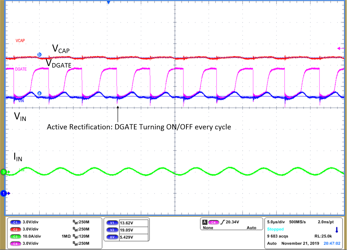
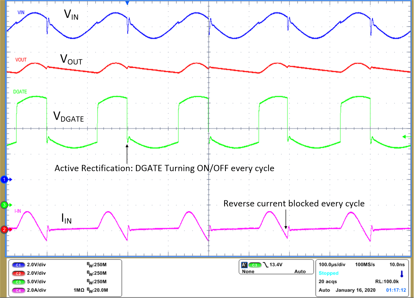
Active rectification of 2-V peak-peak 200 KHz AC input by LM74810-Q1 is shown in Figure 9-3. Fast turn off and quick turn ON of the MOSFET reduces power dissipation in the MOSFET Q1 and active rectification reduces power dissipation in the output hold-up capacitor's ESR by half. Active rectification of 2-V peak-peak 5-KHz AC input is shown in Figure 9-4.
 Figure 9-3 AC Super Imposed Test on 15 nC QGS-
2-V Peak-Peak 200 KHz
 Figure 9-4 AC Super Imposed Test - 2-V Peak-Peak 5
KHz