ZHCSLD2E may 2020 – july 2023 UCC28782
PRODUCTION DATA
- 1
- 1 特性
- 2 应用
- 3 描述
- 4 Revision History
- 5 Device Comparison Table
- 6 Pin Configuration and Functions
- 7 Specifications
-
8 Detailed Description
- 8.1 Overview
- 8.2 Functional Block Diagram
- 8.3
Detailed Pin Description
- 8.3.1 BUR Pin (Programmable Burst Mode)
- 8.3.2 FB Pin (Feedback Pin)
- 8.3.3 REF Pin (Internal 5-V Bias)
- 8.3.4 VDD Pin (Device Bias Supply)
- 8.3.5 P13 and SWS Pins
- 8.3.6 S13 Pin
- 8.3.7 IPC Pin (Intelligent Power Control Pin)
- 8.3.8 RUN Pin (Driver and Bias Source for Isolator)
- 8.3.9 PWMH and AGND Pins
- 8.3.10 PWML and PGND Pins
- 8.3.11 SET Pin
- 8.3.12 RTZ Pin (Sets Delay for Transition Time to Zero)
- 8.3.13 RDM Pin (Sets Synthesized Demagnetization Time for ZVS Tuning)
- 8.3.14 BIN, BSW, and BGND Pins
- 8.3.15 XCD Pin
- 8.3.16 CS, VS, and FLT Pins
- 8.4
Device Functional Modes
- 8.4.1 Adaptive ZVS Control with Auto-Tuning
- 8.4.2 Dead-Time Optimization
- 8.4.3 EMI Dither and Dither Fading Function
- 8.4.4 Control Law across Entire Load Range
- 8.4.5 Adaptive Amplitude Modulation (AAM)
- 8.4.6 Adaptive Burst Mode (ABM)
- 8.4.7 Low Power Mode (LPM)
- 8.4.8 First Standby Power Mode (SBP1)
- 8.4.9 Second Standby Power Mode (SBP2)
- 8.4.10 Startup Sequence
- 8.4.11 Survival Mode of VDD (INT_STOP)
- 8.4.12 Capacitor Voltage Balancing Function
- 8.4.13 Device Functional Modes for Bias Regulator Control
- 8.4.14
System Fault Protections
- 8.4.14.1 Brown-In and Brown-Out
- 8.4.14.2 Output Over-Voltage Protection (OVP)
- 8.4.14.3 Input Over Voltage Protection (IOVP)
- 8.4.14.4 Over-Temperature Protection (OTP) on FLT Pin
- 8.4.14.5 Over-Temperature Protection (OTP) on CS Pin
- 8.4.14.6 Programmable Over-Power Protection (OPP)
- 8.4.14.7 Peak Power Limit (PPL)
- 8.4.14.8 Output Short-Circuit Protection (SCP)
- 8.4.14.9 Over-Current Protection (OCP)
- 8.4.14.10 External Shutdown
- 8.4.14.11 Internal Thermal Shutdown
- 8.4.15 Pin Open/Short Protections
-
9 Application and Implementation
- 9.1 Application Information
- 9.2
Typical Application Circuit
- 9.2.1 Design Requirements for a 65-W USB-PD Adapter Application
- 9.2.2
Detailed Design Procedure
- 9.2.2.1 Input Bulk Capacitance and Minimum Bulk Voltage
- 9.2.2.2 Transformer Calculations
- 9.2.2.3 Clamp Capacitor Calculation
- 9.2.2.4 Bleed-Resistor Calculation
- 9.2.2.5 Output Filter Calculation
- 9.2.2.6 Calculation of ZVS Sensing Network
- 9.2.2.7 Calculation of BUR Pin Resistances
- 9.2.2.8 Calculation of Compensation Network
- 9.2.3 Application Curves
- 10Power Supply Recommendations
- 11Layout
- 12Device and Documentation Support
- 13Mechanical, Packaging, and Orderable Information
8.3.15 XCD Pin
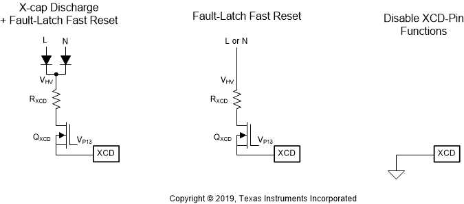
The XCD pin performs X-capacitor discharge and the fault-latch fast-reset functions in conjunction with the recommended external detection circuits, shown in Figure 8-15. The first application circuit allows to perform the two functions at the same time. The second application circuit achieves the fault-latch fast-reset only. The two application circuits must be connected to the AC input but not the DC input, in order to avoid the thermal issue of those sensing components caused by enabling the discharge current repetitively. If neither function is needed, directly shorting the two XCD pins to the AGND pin disables the XCD pin functions, so the controller wait-state current is further reduced. The external sensing circuit must be removed.
 Figure 8-15 XCD-pin Application Circuits
To form the discharge path in the first circuit, the anode nodes of two high-voltage diode rectifiers are connected to each X-cap terminal, the two diode cathodes are connected together to a 26-kΩ current limit resistance (RXCD), and the drain-to-source of a high-voltage depletion MOSFET (QXCD) couples the resistance to XCD pins. Since RXCD needs to sustain the high voltage drop from the XCD-pin current, two series 13-kΩ SMD resistors in 1206 size with 26-kΩ total resistance are required to meet the voltage de-rating. A 600-V rated MOSFET such as BSS126 is needed as the high voltage blocking device. The MOSFET gate is connected to the P13 pin, so the highest voltage level of the XCD pins is limited to the sum of the P13-pin voltage and the threshold voltage of BSS126. The voltage level gives sufficient headroom over the 6.5-V line zero-crossing (LZC) threshold.
In case of single-fault event where one XCD pin is in fail-open condition, the redundant XCD pin helps to maintain the X-cap discharge function. In case of the single-fault event of BSS126 involving its drain-to-source in fail-short condition, an internal 26-V clamp helps to protect the XCD pin from exceeding its voltage rating. The current-limiting resistance (RXCD) limits the fault current below the maximum clamping capability, however the value of RXCD should avoid reducing the normal discharge current. A total resistance of 26 kΩ ±5% meets both criteria. The internal clamping function can also help to dissipate some of the line surge energy accumulated on the XCD pins in order to limit the pin voltage below its 30-V rating.
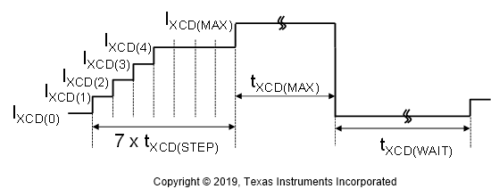
After the AC line is disconnected, X-capacitors in the EMI filters on the AC side of the diode-bridge rectifier must have means to discharge its residual voltage to a safe level within a certain time. Typically a high voltage discharge resistor bank is placed in parallel with the capacitor to form a discharge path. The value of the resistance is chosen to discharge the capacitance within the required time period. However, if the capacitance is large enough, the necessary lower value of discharge resistance will increase the standby power. UCC28782 provides an active X-capacitor discharge function with 2-mA maximum discharge current capability to reduce the standby power. The discharge current is activated only when the detection criteria for the AC-line removal condition is met. The 6.5-V line zero-crossing (LZC) threshold on XCD pins is used to detect AC-line presence. When LZC is missing over an 84-ms detection timeout period, the discharge current is enabled for a maximum period of 300 ms followed by a 700-ms blanking time with no current. To detect the zero crossing reliably, as well as to save power consumption, a stair-case test current shown in Figure 8-16 is generated within the 84-ms detection time. The worst-case discharge current and timing are designed to discharge the X-capacitor up to 1 µF.
 Figure 8-16 Step-current Profile into the XCD Pins for the X-cap Discharge Function
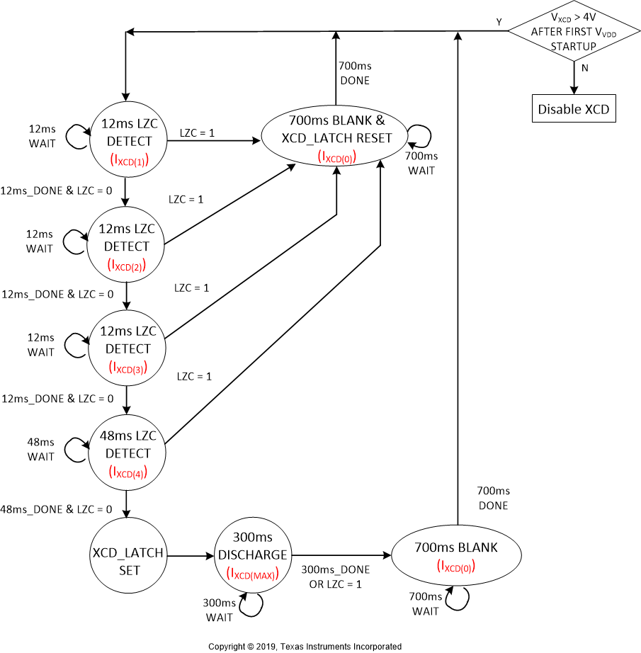
The four test current levels are designed to overcome the impact of leakage current from the bridge diode over a wide line range. Without enough test current level in a 12-ms period, the diode leakage current will prevent the XCD-pin voltage from reaching close to the 6.5-V LZC threshold. A higher AC line voltage or a higher diode junction temperature requires a higher test current due to the increased diode leakage current. When the AC line is connected, the four stair-case current levels and the 700-ms time out after the completion of LZC detection helps to minimize the average current sink from AC main and thereby the static power loss. For the first three current levels, every 12-ms time-out event commands the test current to increment. The last test current level has to be sustained for 48 ms without LZC, before triggering the 2-mA discharge mode. Whenever LZC is detected, any higher-level test-current steps are aborted and the 700-ms wait-state is initiated. Figure 8-17 shows the flow chart of X-capacitor discharge and the fault-latch reset sequence.
Note that the XCD-LATCH referenced in Figure 8-17 is not the same as the Fault-Latch. XCD-LATCH is a latch that is set when loss of AC line is confirmed. When set, this state allows the Fault-Latch to be reset and allows X-capacitor discharge to proceed.
 Figure 8-17 The State Diagram of the XCD-pin Function
Whenever any system protection triggers the fault-latch, the converter switching is terminated and VVDD restart cycle occurs between VVDD(ON) and VVDD(OFF). In this mode, the XCD pin function continues to operate, since the internal circuitry is separately biased from VVDD instead of from VREF. When the AC line is disconnected, the large bulk input capacitor of the ACF prevents VVDD from decaying below the 4.3-V fault reset threshold quickly enough. If the AC line recovers too fast without the XCD pin detection, the controller will still stay in a latched condition and output voltage fails to retry. The two XCD-pin detection circuits can inform the controller the instant of AC line recovery based on the LZC detection concept, so the controller can directly reset the fault condition more quickly.
The second application circuit performs the fault-latch fast-reset without the need for the two high voltage diodes, so essential sensing components become fewer. In the first application circuit with both line and neutral connections, the frequency of the XCD-pin signal is twice the AC-line frequency, and the 12-ms timeout is long enough for VXCD to reach the LZC threshold when the test current becomes sufficient. On the other hand, since the current-limit resistor is connected directly to either line or neutral of the AC input in the second application circuit, only the line-frequency waveform on the XCD pins can trigger the LZC threshold. Because the 12-ms timeout is shorter than a 50-Hz or 60-Hz line cycle, the LZC detection time requires two 12-ms timeout periods to allow the latch reset function to be triggered correctly. Considering the average static current into the XCD pins and the circuit power loss, the second application circuit is lower than the first one. At a high-line condition, the second circuit only needs to use the second step current of 775 µA to detect LZC, while the first circuit may need to increase to the third or fourth step current in order to obtain a valid LZC detection.
Shorting the XCD pins to AGND disables both functions automatically. After VVDD first reaches VVDD(ON), a 80-µA test current is sourced out of the XCD pin, in order to reliably identify the XCD-pin short with a low-impedance path to the AGND pin. If XCD is shorted to AGND, any path to L and N must be open to prevent RXCD from overheating. When VXCD is lower than 4 V before the RUN-pin first pulls high, the function is disabled and the internal circuit will stop sourcing current from VVDD. Different from the first two application circuits, when a latch-off fault happens, the only way to reset the fault condition for this connection is to wait for VVDD to drop below the 4.3-V logic reset threshold (VVDD(RST))) first before the next VVDD restart cycle occurs. With large bulk capacitance, VVDD may cycle for several minutes before its energy is depleted low enough to drop to 4.3V. This connection may be more useful for the all auto-recovery fault setting, or for the latch-off fault setting with no stringent latch reset time limitation.