ZHCSLD2E may 2020 – july 2023 UCC28782
PRODUCTION DATA
- 1
- 1 特性
- 2 应用
- 3 描述
- 4 Revision History
- 5 Device Comparison Table
- 6 Pin Configuration and Functions
- 7 Specifications
-
8 Detailed Description
- 8.1 Overview
- 8.2 Functional Block Diagram
- 8.3
Detailed Pin Description
- 8.3.1 BUR Pin (Programmable Burst Mode)
- 8.3.2 FB Pin (Feedback Pin)
- 8.3.3 REF Pin (Internal 5-V Bias)
- 8.3.4 VDD Pin (Device Bias Supply)
- 8.3.5 P13 and SWS Pins
- 8.3.6 S13 Pin
- 8.3.7 IPC Pin (Intelligent Power Control Pin)
- 8.3.8 RUN Pin (Driver and Bias Source for Isolator)
- 8.3.9 PWMH and AGND Pins
- 8.3.10 PWML and PGND Pins
- 8.3.11 SET Pin
- 8.3.12 RTZ Pin (Sets Delay for Transition Time to Zero)
- 8.3.13 RDM Pin (Sets Synthesized Demagnetization Time for ZVS Tuning)
- 8.3.14 BIN, BSW, and BGND Pins
- 8.3.15 XCD Pin
- 8.3.16 CS, VS, and FLT Pins
- 8.4
Device Functional Modes
- 8.4.1 Adaptive ZVS Control with Auto-Tuning
- 8.4.2 Dead-Time Optimization
- 8.4.3 EMI Dither and Dither Fading Function
- 8.4.4 Control Law across Entire Load Range
- 8.4.5 Adaptive Amplitude Modulation (AAM)
- 8.4.6 Adaptive Burst Mode (ABM)
- 8.4.7 Low Power Mode (LPM)
- 8.4.8 First Standby Power Mode (SBP1)
- 8.4.9 Second Standby Power Mode (SBP2)
- 8.4.10 Startup Sequence
- 8.4.11 Survival Mode of VDD (INT_STOP)
- 8.4.12 Capacitor Voltage Balancing Function
- 8.4.13 Device Functional Modes for Bias Regulator Control
- 8.4.14
System Fault Protections
- 8.4.14.1 Brown-In and Brown-Out
- 8.4.14.2 Output Over-Voltage Protection (OVP)
- 8.4.14.3 Input Over Voltage Protection (IOVP)
- 8.4.14.4 Over-Temperature Protection (OTP) on FLT Pin
- 8.4.14.5 Over-Temperature Protection (OTP) on CS Pin
- 8.4.14.6 Programmable Over-Power Protection (OPP)
- 8.4.14.7 Peak Power Limit (PPL)
- 8.4.14.8 Output Short-Circuit Protection (SCP)
- 8.4.14.9 Over-Current Protection (OCP)
- 8.4.14.10 External Shutdown
- 8.4.14.11 Internal Thermal Shutdown
- 8.4.15 Pin Open/Short Protections
-
9 Application and Implementation
- 9.1 Application Information
- 9.2
Typical Application Circuit
- 9.2.1 Design Requirements for a 65-W USB-PD Adapter Application
- 9.2.2
Detailed Design Procedure
- 9.2.2.1 Input Bulk Capacitance and Minimum Bulk Voltage
- 9.2.2.2 Transformer Calculations
- 9.2.2.3 Clamp Capacitor Calculation
- 9.2.2.4 Bleed-Resistor Calculation
- 9.2.2.5 Output Filter Calculation
- 9.2.2.6 Calculation of ZVS Sensing Network
- 9.2.2.7 Calculation of BUR Pin Resistances
- 9.2.2.8 Calculation of Compensation Network
- 9.2.3 Application Curves
- 10Power Supply Recommendations
- 11Layout
- 12Device and Documentation Support
- 13Mechanical, Packaging, and Orderable Information
8.3.6 S13 Pin
As shown in Power Management Function for a GaN Power IC and PFC Controller, the S13 pin (switched 13-V rail) is used to perform bias-power management for a primary-side GaN power IC, along with an example application where it also powers a PFC controller. This configuration enables to minimize the power-loss contribution to so-called "tiny-load" input power and stand-by power.
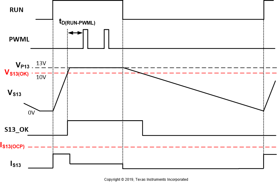
S13 is sourced by P13 through an internal 2.8-Ω switch controlled by the RUN pin. Figure 8-8 illustrates the power-up sequence of the S13 pin. When RUN is high, the S13 decoupling capacitor is charged up to 13 V and the charge current is controlled by an internal soft-start current limiter. The S13-pin voltage must increase above the 10-V power-good threshold (VS13(OK)) in order to initiate PWML switching of each burst cycle. When RUN is low, VS13 is discharged by the loading on S13. The power-on delay of the GaN power IC on the S13 pin must be less than 2 µs to be responsive to PWML. If not, the VDD or P13 pin may be a more suitable bias supply for devices with long power-on delay, but the wait-state power consumption will be compromised. A 22-nF ceramic capacitor as CS13(ZVSF) is recommended. If the S13 pin is not used, it can be connected to the P13 pin in order to eliminate the delay effect on PWML switching in every low-frequency burst cycle.
 Figure 8-7 Power
Management Function for a GaN Power IC and PFC Controller
 Figure 8-8 Power-up Sequence of the S13 Pin
When the S13 pin supplies both the GaN power IC and a PFC controller at the same time, a low-voltage rectifier diode (DS13) between the S13 pin and the PFC controller bias VCC pin is needed, so the local decoupling capacitor for each powered device can be separated. The decoupling capacitor of the PFC controller (CS13(PFC)) is usually larger than the one for a GaN power IC, such that the bias voltage of the GaN power IC will discharge more quickly without affecting the PFC bias voltage and PFC output voltage regulation. If the S13 pin supplies a PFC controller only, the rectifier diode is not needed.
During start-up before VDD reaches the VVDD(ON) threshold, the S13 switch stays off, so the S13-pin loading will not consume any of the charging current of VDD capacitor flowing from SWS pin to VDD pin, thereby enabling a fast start-up sequence. Under this condition, the PFC controller will be off resulting in a lower PFC bus voltage below 400 V.