ZHCSLD2E may 2020 – july 2023 UCC28782
PRODUCTION DATA
- 1
- 1 特性
- 2 应用
- 3 描述
- 4 Revision History
- 5 Device Comparison Table
- 6 Pin Configuration and Functions
- 7 Specifications
-
8 Detailed Description
- 8.1 Overview
- 8.2 Functional Block Diagram
- 8.3
Detailed Pin Description
- 8.3.1 BUR Pin (Programmable Burst Mode)
- 8.3.2 FB Pin (Feedback Pin)
- 8.3.3 REF Pin (Internal 5-V Bias)
- 8.3.4 VDD Pin (Device Bias Supply)
- 8.3.5 P13 and SWS Pins
- 8.3.6 S13 Pin
- 8.3.7 IPC Pin (Intelligent Power Control Pin)
- 8.3.8 RUN Pin (Driver and Bias Source for Isolator)
- 8.3.9 PWMH and AGND Pins
- 8.3.10 PWML and PGND Pins
- 8.3.11 SET Pin
- 8.3.12 RTZ Pin (Sets Delay for Transition Time to Zero)
- 8.3.13 RDM Pin (Sets Synthesized Demagnetization Time for ZVS Tuning)
- 8.3.14 BIN, BSW, and BGND Pins
- 8.3.15 XCD Pin
- 8.3.16 CS, VS, and FLT Pins
- 8.4
Device Functional Modes
- 8.4.1 Adaptive ZVS Control with Auto-Tuning
- 8.4.2 Dead-Time Optimization
- 8.4.3 EMI Dither and Dither Fading Function
- 8.4.4 Control Law across Entire Load Range
- 8.4.5 Adaptive Amplitude Modulation (AAM)
- 8.4.6 Adaptive Burst Mode (ABM)
- 8.4.7 Low Power Mode (LPM)
- 8.4.8 First Standby Power Mode (SBP1)
- 8.4.9 Second Standby Power Mode (SBP2)
- 8.4.10 Startup Sequence
- 8.4.11 Survival Mode of VDD (INT_STOP)
- 8.4.12 Capacitor Voltage Balancing Function
- 8.4.13 Device Functional Modes for Bias Regulator Control
- 8.4.14
System Fault Protections
- 8.4.14.1 Brown-In and Brown-Out
- 8.4.14.2 Output Over-Voltage Protection (OVP)
- 8.4.14.3 Input Over Voltage Protection (IOVP)
- 8.4.14.4 Over-Temperature Protection (OTP) on FLT Pin
- 8.4.14.5 Over-Temperature Protection (OTP) on CS Pin
- 8.4.14.6 Programmable Over-Power Protection (OPP)
- 8.4.14.7 Peak Power Limit (PPL)
- 8.4.14.8 Output Short-Circuit Protection (SCP)
- 8.4.14.9 Over-Current Protection (OCP)
- 8.4.14.10 External Shutdown
- 8.4.14.11 Internal Thermal Shutdown
- 8.4.15 Pin Open/Short Protections
-
9 Application and Implementation
- 9.1 Application Information
- 9.2
Typical Application Circuit
- 9.2.1 Design Requirements for a 65-W USB-PD Adapter Application
- 9.2.2
Detailed Design Procedure
- 9.2.2.1 Input Bulk Capacitance and Minimum Bulk Voltage
- 9.2.2.2 Transformer Calculations
- 9.2.2.3 Clamp Capacitor Calculation
- 9.2.2.4 Bleed-Resistor Calculation
- 9.2.2.5 Output Filter Calculation
- 9.2.2.6 Calculation of ZVS Sensing Network
- 9.2.2.7 Calculation of BUR Pin Resistances
- 9.2.2.8 Calculation of Compensation Network
- 9.2.3 Application Curves
- 10Power Supply Recommendations
- 11Layout
- 12Device and Documentation Support
- 13Mechanical, Packaging, and Orderable Information
8.4.10 Startup Sequence
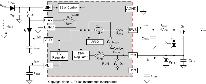
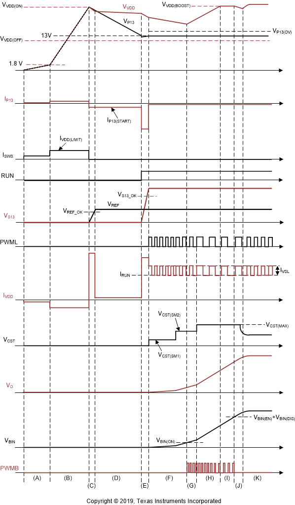
Figure 8-31 shows the simplified block diagram related with the VDD startup function of UCC28782, and Figure 8-32 addresses the startup sequence. The detailed description on the startup waveforms is :
- Time interval A: The UVLO circuit commands the two internal power-path switches (QDDS and QDDP) to close the connections between SWS, VDD, and P13 pins through two serial current-limiting resistors (RDDS and RDDP). The depletion-mode MOSFET (QS) starts sourcing charge current (ISWS) safely from the high-voltage switch-node voltage (VSW) to the VDD capacitor (CVDD). Before VVDD reaches 1.8 V, ISWS is limited by the high-resistance RDDS of 5 kΩ to prevent potential device damage if CVDD or VDD pin is shorted to ground.
- Time interval B: After VVDD rises above 1.8 V, RDDS is reduced to a smaller resistance of 0.5 kΩ. ISWS is increased to charge CVDD faster. The maximum charge current during VDD startup can be quantified by Equation 8.
- Time interval C: As VVDD reaches VVDD(ON) of 17 V, the ULVO circuit turns-off QDDS to disconnect the source pin of QS to CVDD, and turns-off QDDP to break the gate-to-source connection of QS, so QS loses its current-charge capability. VVDD then starts to drop, because the 5-V regulator on REF pin starts to charge up the reference capacitor (CREF) to 5 V, for which the maximum charge current (ISE(REF)) is self-limited at around 17 mA. After VREF is settled, the UVLO circuit turns-on another power-path switch (QP13), so an internal 13-V regulator is connected to the P13 pin. The voltage on the P13 pin capacitor (CP13) starts to be discharged by the regulator.
- Time interval D: While discharging the recommended 1 µF on CP13 , the sink current of the 13-V regulator (IP13(START)) is self-limited at around 2.2 mA, so it takes longer than 10 μs to settle to 13 V. If VP13 reaches 13 V in less than 10 μs, the P13 pin open fault is triggered to protect the device. Once VP13 has settled to 13 V without the fault event, RUN pin goes high and UCC28782 enters a run state with IVDD = IRUN.
- Time interval E: There is a minimum 2.2-μs delay from RUN going high to PWML starting to switch in order to wake-up the gate driver and UCC28782. In this interval, the 2.8-Ω power path switch between the P13 pin and the S13 pin is enabled, so the S13-pin decoupling capacitor (CS13) is charged up and the charge current is supplied from CP13 and the P13 regulator. If 2.2-μs delay is timed out before VS13 reaches to the 10-V power good threshold (VS13_OK), the PWML switching instance will be further delayed.
- Time interval F: This is the soft-start region of peak magnetizing current. The first purpose is to limit the supply current if the output is short. The second purpose is to push the switching frequency higher than the audible frequency range during repetitive startup situations. At the beginning of VO soft-start, the peak current is limited by two VCST thresholds. The first VCST startup threshold (VCST(SM1)) is clamped at 0.2 V and the following second threshold (VCST(SM2)) is 0.5 V. When VCST = VCST(SM1), PWMH is disabled if the sampled VS pin voltage (VVS) < 0.28 V, and the first five PWML pulses are forced to stay at this current level. After the sampled VVS exceeds 0.28 V and the first five PWML pulses are generated, the peak current threshold changes from VCST(SM1) to VCST(SM2). In case of the inability to build up VO with VCST(SM1) at the beginning of the VO soft-start due to excessively large output capacitor and/or constant-current output load, there is an internal time-out of 0.7 ms to force VCST to switch to VCST(SM2). At this moment, the BIN-pin capacitor voltage increases with VO proportionally. If VBIN is less than the 2.2-V UVLO threshold (VBIN(ON)), the bias switching regulator is disabled.
- Time interval G: When VBIN is higher than 2.2 V, the bias switching regulator enters into the boost switching mode, and starts to build up the VVDD toward the 18.5-V regulation level.
- Time interval H: When VVS rises above 0.5 V, VCST is allowed to reach VCST(MAX) , so the ramp rate of VO startup becomes faster. When PWML is in a high state, IVDD can be larger than IRUN, because the 5-V regulator provides the line-sensing current pulse (IVSL) on the VS pin to sense VBULK condition.
- Time interval I: Higher VBIN results in a lower switching frequency of the bias regulator, because more energy in the boost inductor (LB) is transferred to CVDD every switching cycle.
- Time interval J: When VBIN increases above the 15-V boost disable threshold, the VVDD starts to decay back to the rectified auxiliary winding voltage minus the forward voltage drop of the boost diode (DB). Also, when VO gets close to the target regulation level, VCST starts to reduce from VCST(MAX).
- Time interval K: VO and VCST settle, and the auxiliary winding takes over the VDD supply.
 Figure 8-31 Functional Startup Block Diagram
 Figure 8-32 Startup Timing Waveforms